
Phase Shifted Full Bridge Converter
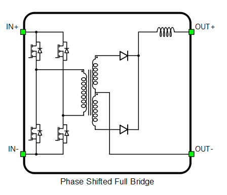
Description of the Phase Shifted Full Bridge component in Schematic Editor
Solver platform
- UltraCore: Default option, which utilizes UltraCore to simulate the converter with enhanced resolution, using UltraCore step. UltraCore weight of the component is 3.
- SPC: Simulates the converter using SPC resources, with a simulation timestep equal to the rest of the electrical model. SPC weight of the component is 3.
When the switching frequency is higher than 100 kHz, the usage of UltraCore is advised.
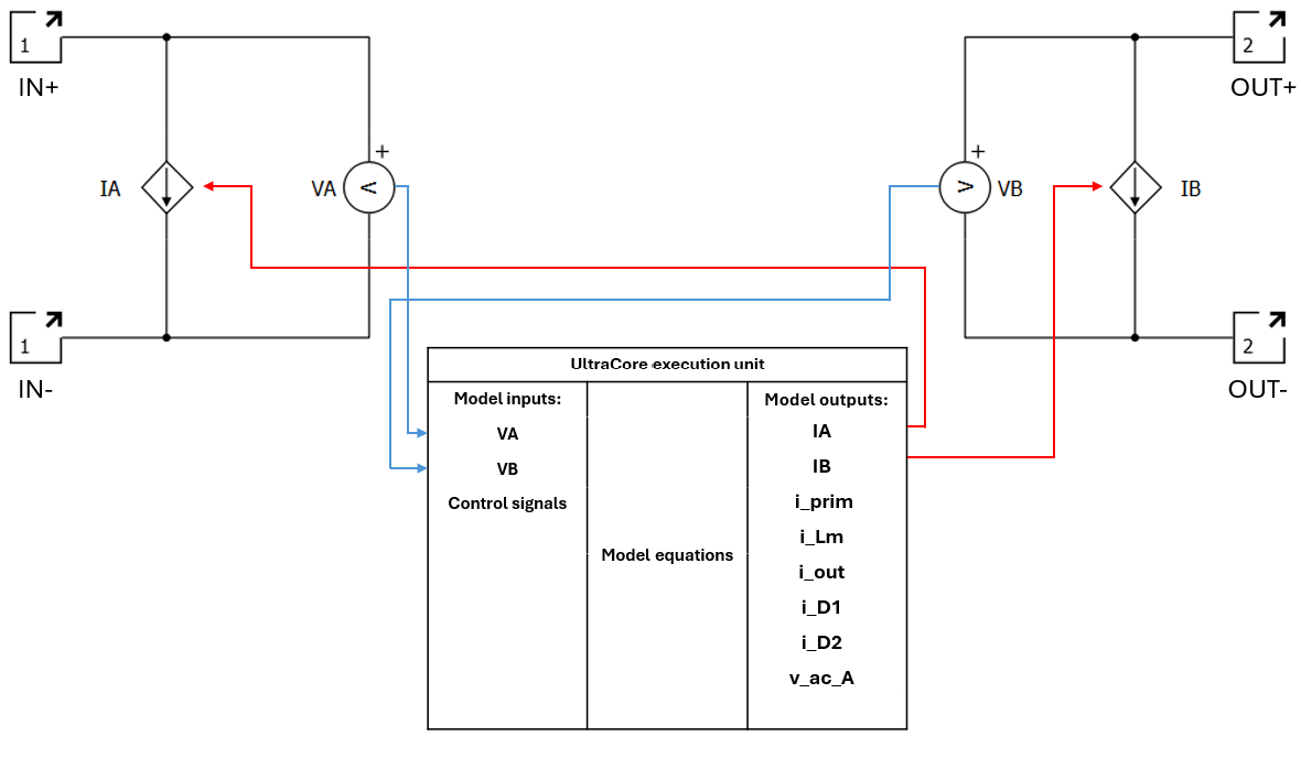
If UltraCore is selected as the solver platform, the component will contain an interfacing electrical circuit towards the rest of the circuit, as described in Electrical circuit interface. The Phase Shifted Full Bridge component in the Typhoon HIL Schematic Editor Library uses the current source interface. The interface is formulated in such a way that the voltages are inputs to the dedicated UltraCore, while the currents are its outputs. Figure 2 shows the circuit interface of the Phase Shifted Full Bridge converter component.
If SPC is selected for real-time/VHIL simulations, this converter requires a device configuration that supports Switch-level GDS oversampling.
Schematic Block Diagram
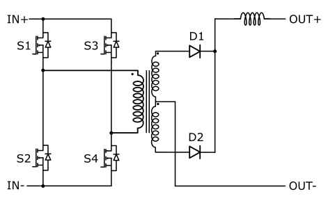
The schematic block diagram of the Phase Shifted Full Bridge converter component differs depending on the selected Rectifier topology, Active rectification and Solver platform. When SPC is used, only Center-tapped passive rectifier is supported. A schematic block diagram with corresponding switch naming when the SPC platform is used is given in Figure 3.
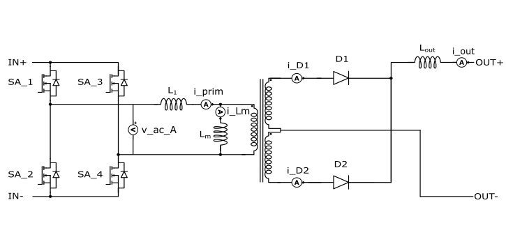
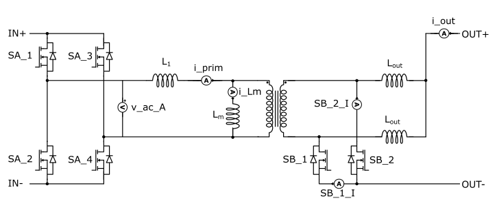
When UltraCore is used, three rectifier topology options are available: Center-tapped, Full bridge and Current doubler. For all options, both passive and active realizations are supported. Schematic block diagrams with corresponding switch naming when the Active rectification property is disabled are given in Figure 4, Figure 5, and Figure 6.
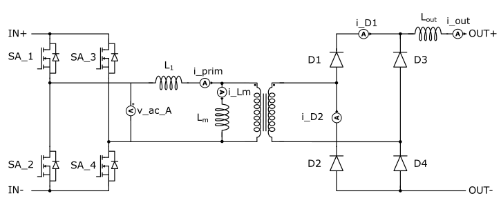
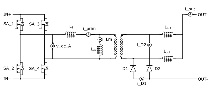
Schematic block diagrams with corresponding switch naming when the Active rectification property is enabled are given in Figure 7, Figure 8, and Figure 9.
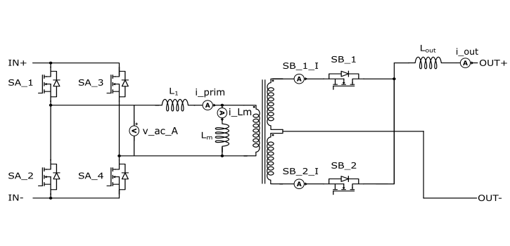
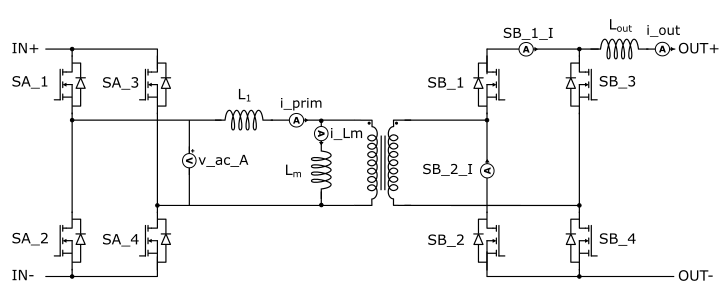
Control
Selecting Digital inputs as the Control parameter enables assigning gate drive inputs to any of the digital input pins (from 1 to 32(64)). For example, if SA_1 is assigned to 1, the digital input pin 1 will be routed to the SA_1 switch gate drive. In addition, the gate_logic parameter selects either active high (High-level input voltage VIH turns on the switch), or active low (Low-level input voltage VIL turns on the switch) gate drive logic, depending on the design of the external controller. In TyphoonSim, digital signals are read from the internal virtual IO bus. Hence, if some signal is sent to digital ouput 1, it will appear on digital input 1.
Selecting Internal modulator as the Control parameter enables use of the internal PWM modulator for driving SA_1, SA_2, SA_3, and SA_4 switches instead of the digital input pins. In this configuration, three additional component inputs will be present. En input is used to enable/disable the internal PWM modulator, while InA and InB are used as reference signal inputs. When options for variable frequency or phase are selected, additional component inputs are created: Freq, OffsetA, and OffsetB respectively.
Model control option is available only when SPC is selected as Solver platform. Selecting Model as the Control parameter enables setting the IGBTs' gate drive signals directly from the signal processing model. The input pin gates appears on the component and requires a vector input of four gate drive signals in the following order: [SA_1, SA_2, SA_3, SA_4]. When controlled from the model, logic is always active high.
Analog output variable naming for the Phase Shifted Full Bridge switching block (internal to the component)
| Analog output variable name | Description |
|---|---|
| i_prim | Current of primary side leakage inductance. |
| i_Lm | Current of magnetizing inductance of the transformer. Available if Center- tapped or Full bridge secondary topology is used. |
| i_out | Current of output inductance. |
| i_D1 | Diode D1 current when Active rectification is disabled. Available if UltraCore is used. |
| i_D2 | Diode D2 current when active rectification is disabled. Available if UltraCore is used. |
| SB_1_I | Current through switch SB_1 when Active rectification is used. Available if UltraCore is used. |
| SB_2_I | Current through switch SB_2 when Active rectification is used. Available if UltraCore is used. |
| v_ac_A | AC voltages for sides A. |
Digital Alias
If a converter is controlled by digital inputs, an alias for every digital input used by the converter will be created. Digital input aliases will be available under the Digital inputs list alongside existing Digital input signals. The alias will be shown as Converter_name.Switch_name, where Converter_name is name of the converter component and Switch_name is name of the controllable switch in the converter.
Ports
- IN+ (electrical)
- IN side + port.
- IN- (electrical)
- IN side - port.
- OUT+ (electrical)
- OUT side + port.
- OUT- (electrical)
- OUT side - port.
- s_ctrl (in)
- Available if Model control is selected
- Vector of 4 input gate signals for switches
- En (in)
- Available if Internal modulator control is selected
- Used to enable/disable the internal modulator
- InA (in)
- Available if Internal modulator control is selected
- Used to specify modulation signal value for internal modulator leg A, switches SA_1 and SA_2
- InB (in)
- Available if Internal modulator control is selected
- Used to specify modulation signal value for internal modulator leg B, switches SA_3 and SA_4
- Freq (in)
- Available if Internal modulator control is selected and Variable carrier frequency is selected as the modulator's operation mode
- Used to specify modulator's carrier frequency
- OffsetA (in)
- Available if Internal modulator control is selected and Variable carrier phase offset is selected as the modulator's phase operation mode
- Used to specify leg A modulator's carrier phase offset
- OffsetB (in)
- Available if Internal modulator control is selected and Variable carrier phase offset is selected as the modulator's phase operation mode
- Used to specify leg B modulator's carrier phase offset
General (Tab)
- Control
- Specifies how switches are controlled. Available options are: Digital inputs, Internal modulator, and Model
- More details about each type of control can be found in the Control section
- If Digital inputs is selected as Control, the following
properties can be used:
- SA_1
- Digital input that is used to control the SA_1 switch
- SA_1_logic
- Logic that will be applied to control the signal for SA_1
- Active high or active low
- SA_2
- Digital input that is used to control the SA_2 switch
- SA_2_logic
- Logic that will be applied to control the signal for SA_2
- Active high or active low
- SA_3
- Digital input that is used to control the SA_3 switch
- SA_3_logic
- Logic that will be applied to control the signal for SA_3
- Active high or active low
- SA_4
- Digital input that is used to control the SA_4 switch
- SA_4_logic
- Logic that will be applied to control the signal for SA_4
- Active high or active low
- SB_1
- Available if Active rectification is used
- Digital input that is used to control the SB_1 switch
- SB_1_logic
- Available if Active rectification is used
- Logic that will be applied to control the signal for SB_1
- Active high or active low
- SB_2
- Available if Active rectification is used
- Digital input that is used to control the SB_2 switch
- SB_2_logic
- Available if Active rectification is used
- Logic that will be applied to control the signal for SB_2
- Active high or active low
- SB_3
- Available if Active rectification is used and Full bridge rectifier is selected
- Digital input that is used to control the SB_3 switch
- SB_3_logic
- Available if Active rectification is used and Full bridge rectifier is selected
- Logic that will be applied to control the signal for SB_3
- Active high or active low
- SB_4
- Available if Active rectification is used and Full bridge rectifier is selected
- Digital input that is used to control the SB_4 switch
- SB_4_logic
- Available if Active rectification is used and Full bridge rectifier is selected
- Logic that will be applied to control the signal for SB_4
- Active high or active low
- Gate control enabling -A
- If enabled, gives a possibility to control if changes in the gate control signal are applied or not for switches on side A
- Sen -A
- Available if Gate control enabling -A is enabled
- Digital input that enables/disables switching for side A
- Sen_logic -A
- Available if Gate control enabling -A is enabled
- Logic that will be applied to Sen -A signal
- Gate control enabling -B
- If enabled, gives a possibility to control if changes in the gate control signal are applied or not for switches on side B
- Sen -B
- Available if Gate control enabling -B is enabled
- Digital input that enables/disables switching for side B
- Sen_logic -B
- Available if Gate control enabling -B is enabled
- Logic that will be applied to Sen -B signal
- SA_1
- If Model is selected as Control,
the following properties can be used:
- Execution rate
- Defines the period between two updates of gate signals for the component. Gate signals are provided as a signal processing input to component.
- Execution rate
- If Internal modulator is selected as Control, the following
properties can be used:
- Operation mode
- Specifies the source of the internal modulator carrier frequency
- If Operation mode is Fixed carrier frequency, then the frequency can be specified in the component properties
- If Operation mode is Variable carrier frequency, then the frequency can be specified using a signal processing port that appears on the component.
- Carrier frequency (Hz)
- Available if the Operation mode is Fixed carrier frequency
- Specifies the internal modulator's carrier frequency
- Phase operation mode
- Specifies the source of the internal modulator carrier offset
- If Phase operation mode is Fixed carrier phase offset, then the offset can be specified in the component properties
- If Phase operation mode is Variable carrier phase offset, then the offset can be specified using a signal processing port that appears on the component
- Carrier phase offset
- Specifies the internal modulator's carrier phase offset in degrees.
- Vector containing two values: phase offset of leg A, followed by phase offset of leg B.
- Dead time period
- Specifies dead time period for the internal modulator in seconds
- Reference signal [min, max]
- Specifies carrier signal minimal and maximal value
- Vector containing two values: the minimal carrier signal value, followed by the maximal carrier signal value
- Load mode
- Specifies on which event the new value of the modulation signal will be applied
in the internal modulator
- If on min is selected, the new value will be applied when carrier reaches minimal value
- If on max is selected, the new value will be applied when carrier reaches maximal value
- If on either is selected, the new value will be applied when carrier reaches minimal or maximal value
- Specifies on which event the new value of the modulation signal will be applied
in the internal modulator
- Execution rate
- Defines the period between two updates of gate signals for the component. Gate signals are provided as a signal processing input to component
- Operation mode
Electrical (Tab)
- Rectifier topology
- Available if UltraCore is selected as Solver platform.
- Specifies the topology of secondary rectifier. Available options are Center-tapped, Full bridge and Current doubler.
- Active rectification
- Available if UltraCore is selected as Solver platform.
- Specifies how the rectifier will be implemented: passive rectifier (diodes) if not enabled, or active rectifier (transistors) if enabled.
- n1
- Specifies number of turns of the primary winding
- n2
- Specifies number of turns of the secondary winding
- L1
- Specifies leakage inductance of the primary winding
- R1
- Specifies the primary winding resistance
- L2
- Available if SPC is selected as Solver platform.
- Specifies leakage inductance of the secondary winding(s)
- R2
- Specifies the secondary winding resistance(s)
- Lm
- Specifies magnetization inductance
- Rm
- Available if SPC is selected as Solver platform.
- Specifies equivalent resistance representing the iron core losses
- Lout
- Specifies output inductor inductance
Solver (Tab)
- Solver platform
- Select on which platform the converter block will be simulated: SPC or UltraCore
Extras (Tab)
- Public - Components marked as public expose their signals on all levels.
- Protected - Components marked as protected will hide their signals to components outside of their first locked parent component.
- Inherit - Components marked as inherit will take the nearest parent 'signal_access' property value that is set to a value other than inherit.