Resonant Converter
Description of the Resonant Converter component in Schematic Editor.
Schematic Block Diagrams
The Resonant Converter component supports two main topologies: CLLLC Resonant Converter and LLC Resonant Converter.
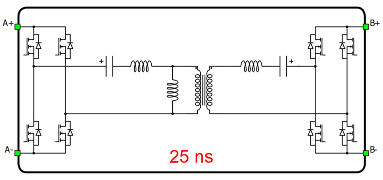
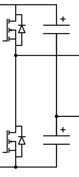
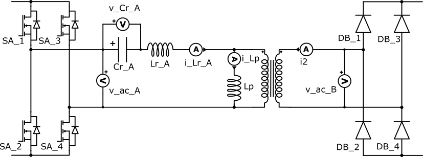
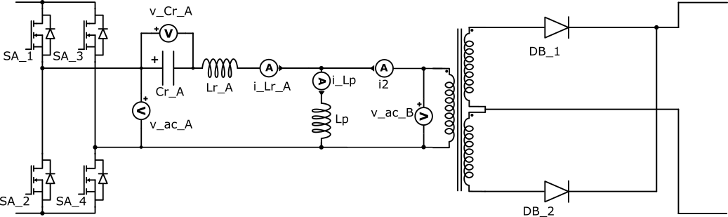
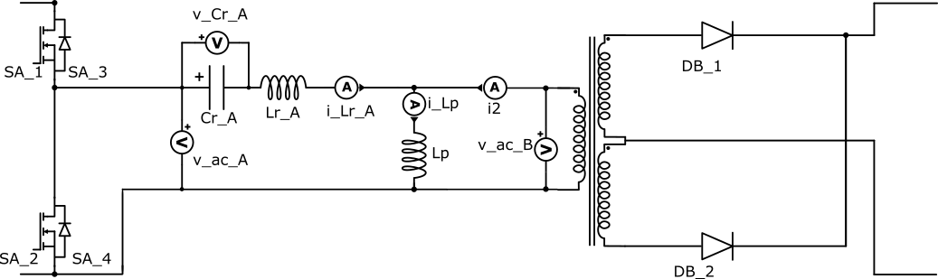
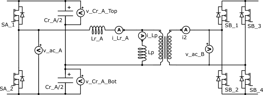
A schematic block diagram of the CLLLC Resonant Converter with corresponding switch naming is given in Figure 2.
In real-time simulation, this converter block uses the dedicated UltraCore FPGA hardware resource in order to achieve a reduced simulation step for this topology.
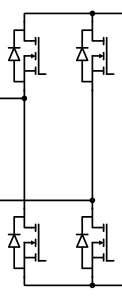
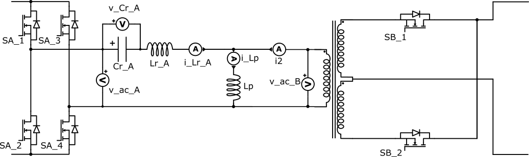
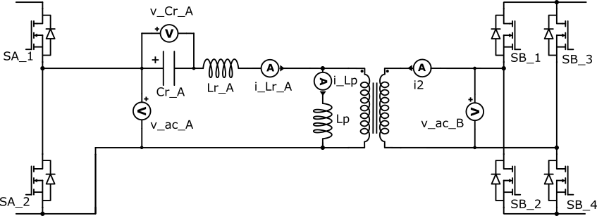
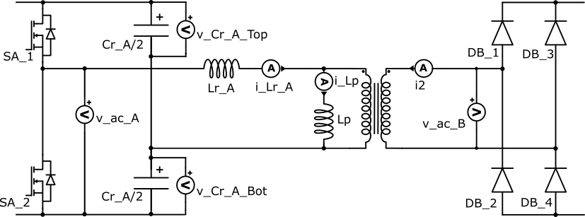
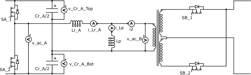
A schematic block diagram of the LLC Resonant Converter with corresponding switch naming is given in Figure 3.
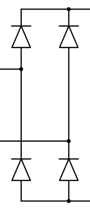
If LLC is selected as the Resonant tank, different A and B side topologies can be selected. Table 1 gives an overview of A side topologies, while Table 2 gives an overview of B side topologies.
| Name | Topology |
|---|---|
|
H-bridge |
|
|
Half bridge |
|
|
Half bridge split-caps |
|
| Name | Topology |
|---|---|
|
H-bridge |
|
|
Full bridge rectifier |
|
|
Active Center-tapped |
|
|
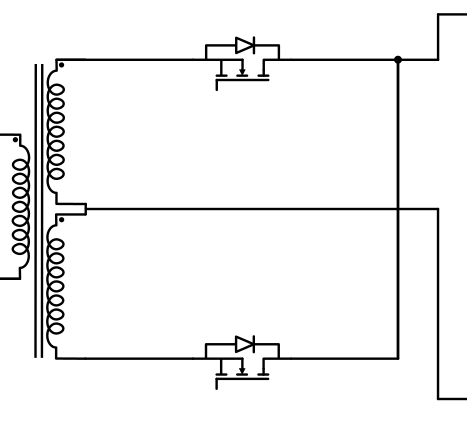
Diode Center-tapped |
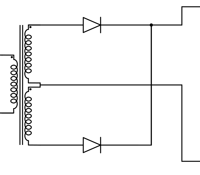
|
Control
Selecting Digital inputs as the Control parameter enables assigning gate drive inputs to any of the digital input pins (from 1 to 32(64)). For example, if SA_1 is assigned to 1, the digital input pin 1 will be routed to the SA_1 switch gate drive. In addition, the gate_logic parameter selects either active high (High-level input voltage VIH turns on the switch), or active low (Low-level input voltage VIL turns on the switch) gate drive logic, depending on the design of the external controller. In TyphoonSim, digital signals are read from the internal virtual IO bus. Hence, if some signal is sent to digital ouput 1, it will appear on digital input 1.
Selecting Internal modulator as the Control parameter, enables use of the internal PWM modulator for driving switches instead of digital input pins.
- In case of CLLLC Resonant Converter, in this configuration, ten additional component inputs will be present. En_A and En_B input is used to enable/disable switching at corresponding side. In_a1, In_a2, In_b1, and In_b2 are used as referent signal inputs for the corresponding internal PWM modulator in legs A1, A2, B1, and B2, respectively. Additionally, Offset_a1, Offset_a2, Offset_b1, and Offset_b2 are used as carrier offsets for the corresponding internal PWM modulator in legs A1, A2, B1, and B2, respectively. If Variable carrier frequency is selected as the Operation mode for the Resonant Converter's internal modulator, an additional port Freq will be present. This port is used as a frequency input for the internal PWM modulator.
- In case of LLC Resonant Converter, in this configuration, Internal modulator drives only switches at A side, while controllable switches at B side (if any exists in selected B topology) will be turned off, so the B side will behave as completely passive. In this configuration, five additional component inputs will be present. En input is used to enable/disable switching. In_a1 and In_a2 are used as referent signal inputs for the corresponding internal PWM modulator in legs A1 and A2, respectively. Additionally, Offset_a1 and Offset_a2 are used as carrier offsets for the corresponding internal PWM modulator in legs A1 and A2, respectively. If the A side topology is not H-bridge, In_a2 and Offset_a2 will not exist. If Variable carrier frequency is selected as the Operation mode for the Resonant Converter's internal modulator, an additional port Freq will be present. This port is used as a frequency input for the internal PWM modulator.
Extras
In real-time simulation, Short-circuit resistance - A and Short-circuit resistance - B are used to define the resistance that will be taken into consideration if some of the legs goes to short-circuit mode. Short-circuits are modelled using short-circuit resistance, which means that if a leg is in short-circuit mode, current drawn from its corresponding DC side will be Vdc_A(B)/Short-circuit resistance - A(B), where Vdc_A(B) is the DC voltage of the corresponding DC side.
Model description in real-time simulation
In real-time simulation, the Resonant Converter runs on UltraCore, a dedicated hardware solver module, which is highly optimized to simulate the dynamics of fast-switching converter topologies with enhanced resolution. This means that the Resonant Converter block does not utilize the same resources that are typically used for other converter blocks, so the weight of the Resonant Converter is 0.
Electrical circuit interface in real-time simulation
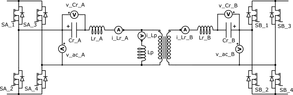
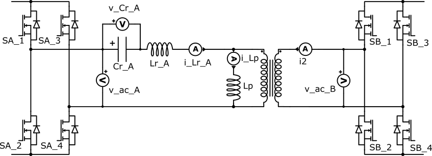
In real-time simulation every component that uses the UltraCore hardware resource contains an interfacing electrical circuit towards the rest of the circuit, as described in Electrical circuit interface. The Resonant Converter component in the Typhoon HIL Schematic Editor Library uses the current source interface. The interface is formulated in such a way that the voltages are inputs to the dedicated UltraCore, while the currents are its outputs. Figure 4 shows the circuit interface of the Resonant Converter comoponent. Model outputs depend on the selected values of properties located in Electrical (Tab) .
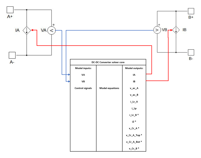
Besides IA and IB which directly affect the surrounding circuit, there are additional component outputs that represent internal electrical measurements. Table 3 shows measurements available depending on the topology. Signals that end in ".cmp_out" are digital comparator signals that compare the analog signals to zero using a greater or equal operator, and are updated at solver step rate.
| Resonant tank | A side topology | B side topology | Measurements |
|---|---|---|---|
|
CLLLC |
H-bridge |
H-bridge |
i_Lr_A, i_Lr_A_cmp_out, i_Lr_B, i_Lr_B_cmp_out, i_Lp, v_Cr_A, v_Cr_B, v_ac_A, v_ac_B |
|
LLC |
H-bridge, Half bridge |
all |
i_Lr_A, i_Lr_A_cmp_out, i2, i2_cmp_out, i_Lp, v_Cr_A, v_ac_A, v_ac_B |
|
LLC |
Half bridge split-cap |
all |
i_Lr_A, i_Lr_A_cmp_out, i2, i2_cmp_out, i_Lp, v_Cr_A_Top, v_Cr_A_Bot, v_ac_A, v_ac_B |
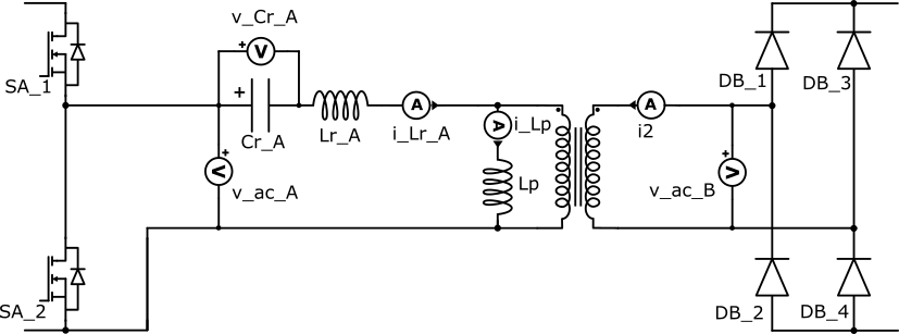
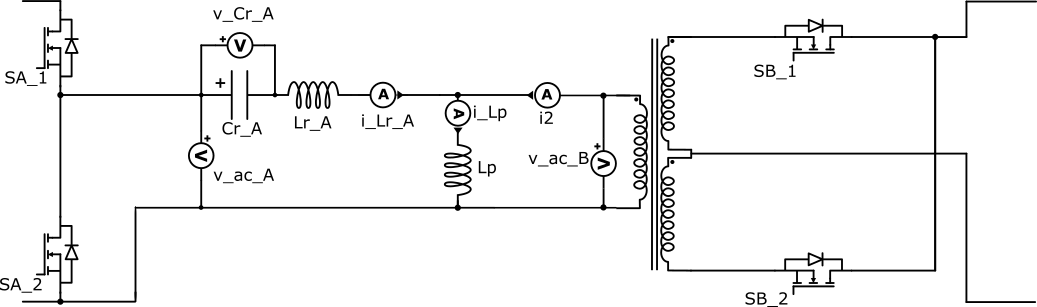
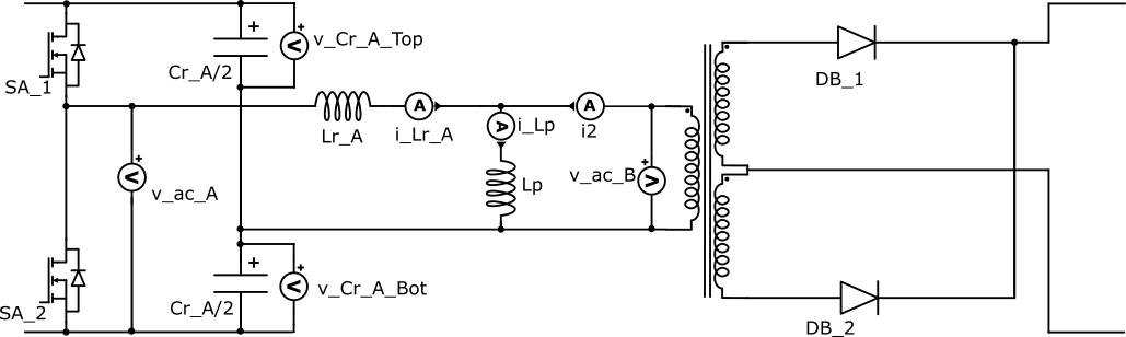
Placement of all measurements for all topologies is shown in the Block diagram(s) of a Resonant Converter component with corresponding switch naming section.
Block diagram(s) of a Resonant Converter component with corresponding switch naming
This section contains a Block diagram of the Resonant Converter component with corresponding switch naming for every combination of A side topology and B side topology for the LLC Resonant converter, as well as the block diagram for the CLLLC Resonant Converter.
Digital Alias
If a converter is controlled by digital inputs, an alias for every digital input used by the converter will be created. Digital input aliases will be available under the Digital inputs list alongside existing Digital input signals. The alias will be shown as Converter_name.Switch_name, where Converter_name is name of the converter component and Switch_name is name of the controllable switch in the converter.
Ports
- A+ (electrical)
- DC side A+ port.
- A- (electrical)
- DC side A- port.
- B+ (electrical)
- DC side B+ port.
- B- (electrical)
- DC side B- port.
Control (Tab)
- Control
- Specifies how switches are controled. It is possible to choose between: Digital inputs and Internal modulator
- More details about each type of control can be found in the Control section
- If Digital inputs is selected as Control, the following
properties can be used:
- SA_1
- Digital input that is used to control SA_1 switch
- SA_1_logic
- Logic that will be applied to control signal for SA_1
- Active high or active low
- SA_2
- Digital input that is used to control SA_2 switch
- SA_2_logic
- Logic that will be applied to control signal for SA_2
- Active high or active low
- SA_3
- Digital input that is used to control SA_3 switch
- SA_3_logic
- Logic that will be applied to control signal for SA_3
- Active high or active low
- SA_4
- Digital input that is used to control SA_4 switch
- SA_4_logic
- Logic that will be applied to control signal for SA_4
- Active high or active low
- SB_1
- Digital input that is used to control SB_1 switch
- SB_1_logic
- Logic that will be applied to control signal for SB_1
- Active high or active low
- SB_2
- Digital input that is used to control SB_2 switch
- SB_2_logic
- Logic that will be applied to control signal for SB_2
- Active high or active low
- SB_3
- Digital input that is used to control SB_3 switch
- SB_3_logic
- Logic that will be applied to control signal for SB_3
- Active high or active low
- SB_4
- Digital input that is used to control SB_4 switch
- SB_4_logic
- Logic that will be applied to control signal for SB_4
- Active high or active low
- Gate control enabling -A
- If enabled, gives a possibility to control if changes in the gate control signal are applied or not for converter A
- Sen -A
- Available if Gate control enabling -A is enabled
- Digital input that enables/disables switching for converter A
- Sen_logic -A
- Available if Gate control enabling -A is enabled
- Logic that will be applied to Sen -A signal
- Gate control enabling -B
- If enabled, gives a possibility to control if changes in the gate control signal are applied or not for converter B
- Sen -B
- Available if Gate control enabling -B is enabled
- Digital input that enables/disables switching for converter B
- Sen_logic -B
- Available if Gate control enabling -B is enabled
- Logic that will be applied to Sen -B signal
- SA_1
- If Internal modulator is selected as Control, the following
properties can be used:
- Operation mode
- Specifies the source of the internal modulator carrier frequency
- If Operation mode is Fixed carrier frequency, then frequency can be specified on the component properties
- If Operation mode is Variable carrier frequency, then the frequency can be specified using a signal processing port
- Carrier frequency (Hz)
- Available if the Operation mode is a Fixed carrier frequency
- Specifies the internal modulator's carrier frequency
- Dead time
- Specifies dead time for the internal modulator in seconds
- Reference signal [min, max]
- Specifies carrier signal minimal and maximal value
- Vector containing two values: the minimal carrier signal value, followed by the maximal carrier signal value
- Load mode
- Specifies on which event the new value of the modulation signal will be applied
in the internal modulator
- If on min is selected, new value will be applied when carrier reaches minimal value
- If on max is selected, new value will be applied when carrier reaches maximal value
- If on either is selected, new value will be applied when carrier reaches minimal or maximal value
- Specifies on which event the new value of the modulation signal will be applied
in the internal modulator
- Operation mode
Electrical (Tab)
- Resonant tank
- Type of Resonant Converter tank - LLC or CLLLC.
- A side topology
- Converter topology at A side
- If CLLLC is selected, only H-bridge is available
- If LLC is selected, H-bridge, Half-bridge, and Half-bridge split-cap are available
- B side topology
- Converter topology at B side
- If CLLLC is selected, only H-bridge is available
- If LLC is selected, H-bridge, Full bridge rectifier, Active center-tapped, and Diode center-tapped are available
- Series inductance (A)
- Series Resonant inductance at A side
- Capacitance (A)
- Series Resonant capacitance at A side. If the Half bridge split-cap topology is selected, this property represents total capacitance of both capacitors at the A side.
- Parallel inductance
- Inductance of parallel inductor
- R series (A)
- Series winding resistance at A side. Rds(on) of switches can be included in this resistance.
- Series inductance (B)
- Series Resonant inductance at B side
- Available if CLLLC Resonant tank is selected
- Capacitance (B)
- Series Resonant capacitance at B side.
- Available if CLLLC Resonant tank is selected
- R series (B)
- Series winding resistance at B side. Rds(on) of switches can be included in this resistance.
- Transformer turns ratio (B/A)
- Defines internal transformer ratio between sides B and A. If the Center-tapped topology is selected, all secondary windings are considered as same and B represents number of turns of single winding.
Extras (Tab)
- Short-circuit resistance - A
- Resistance for side A used to calculate short circuit current if side A is shorted
 This property is not
supported in TyphoonSim. Changing its value will not affect TyphoonSim simulation at
all.
This property is not
supported in TyphoonSim. Changing its value will not affect TyphoonSim simulation at
all.
- Short-circuit resistance - B
- Resistance for side B used to calculate short circuit current if side B is shorted
- This property is not
supported in TyphoonSim. Changing its value will not affect TyphoonSim simulation at
all.
- Public - Components marked as public expose their signals on all levels.
- Protected - Components marked as protected will hide their signals to components outside of their first locked parent component.
- Inherit - Components marked as inherit will take the nearest parent 'signal_access' property value that is set to a value other than inherit.