Grid Commutated 2L Cell
Description of the Grid Commutated 2L Cell converter component in Schematic Editor
Schematic Block Diagram
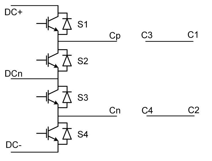
A schematic block diagram of the Commuted 2L Cell block is given in Figure 1 with its corresponding switch arrangement and naming.
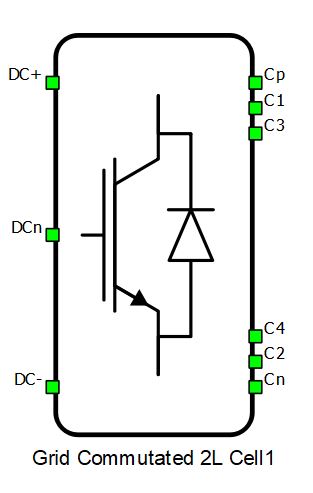
A block diagram and input parameters for the Grid Commutated 2L Cell converter are given in Table 1.
| Component | Component dialog window | Component properties |
|---|---|---|
 |
 |
|
Control
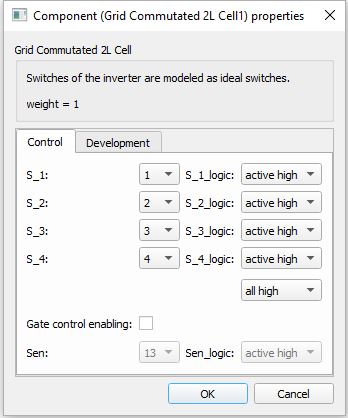
Gate drive inputs can be assigned to any of the digital input pins. For example, if S_1 is set to 1, the digital input pin 1 will be routed to the S1 switch gate. In addition, the S_1_logic parameter selects either active high (High-level input voltage VIH turns on the switch), or active low (Low-level input voltage VIL turns on the switch) gate logic, depending on the external controller design.
Digital Alias
If a converter is controlled by digital inputs, an alias for every digital input used by the converter will be created. Digital input aliases will be available under the Digital inputs list alongside existing Digital input signals. The alias will be shown as Converter_name.Switch_name, where Converter_name is name of the converter component and Switch_name is name of the controllable switch in the converter.