XY Converter
Description of the XY Converter component in Schematic Editor, which can be modified to represent the whole family of XY converters.
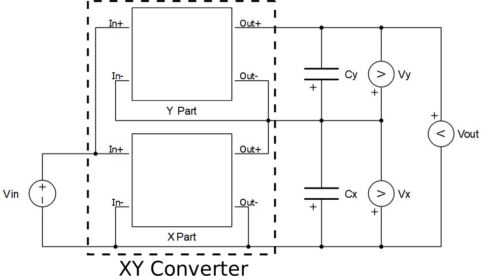
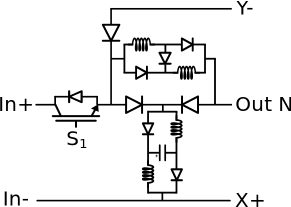
Schematic Block Diagram
A block diagram and input parameters for the XY Converter switching block are given in Table 1.
| component | component dialog window | component parameters |
|---|---|---|

|
|
|
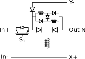
XY Converter basics
As the name suggests, XY Converter consists of two parts: an X and a Y part. Each of the parts behaves similarly to a conventional buck-boost converter. However, with this specific connection, the input voltage of the Y part of the converter is equal to the sum of the input voltage and output voltage of the X part of the XY Converter. This allows for cascade voltage amplification. The output of the XY Converter is actually the sum of the outputs of the X and Y parts of the converter.
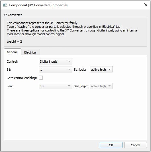
Component dialogue box and parameters
- The General tab contains control-related properties. A detailed description can be seen in Control options.
- Electrical tab parameters are shown in Table 2.
Table 2. Electrical tab properties Property Code name Description X inductance x_inductance Inductance value of a single inductor in the X part of the converter. [H] X inductance type x_ind_type Choose the type of inductance in the X part of the converter. X inductor initial current x_init_current Initial current of the inductor(s) in the X part of the converter. [A] X capacitor capacitance x_capacitance Capacitance value of the capacitor in the X part of the converter, if there is one. [F] X capacitor's ESR x_esr Value of the equivalent series resistance (ESR) of the capacitor in the X part of the converter, if there is one. [Ω] X capacitor's initial voltage x_init_voltage Value of the initial voltage of the capacitor in the X part of the converter, if there is one. [V] Y inductance y_inductance Inductance value of a single inductor in the Y part of the converter. [H] Y inductance type y_ind_type Choose the type of the inductance in the Y part of the converter. Y inductor initial current y_init_current Initial current of the inductor(s) in the Y part of the converter. [A] Y capacitor capacitance y_capacitance Capacitance value of the capacitor in Y part of the converter, if there is one. [F] Y capacitor's ESR y_esr Value of the equivalent series resistance (ESR) of the capacitor in the Y part of the converter, if there is one. [Ω] Y capacitor's initial voltage y_init_voltage Value of the initial voltage of the capacitor in the Y part of the converter, if there is one. [V]
Control options
Selecting Digital inputs as the Control parameter enables assigning gate drive inputs to any of the digital input pins (from 1 to 32(64)). For example, if S1 is assigned to 1, the digital input pin 1 will be routed to the S1 switch gate drive. In addition, the gate_logic parameter selects either active high (High-level input voltage VIH turns on the switch), or active low (Low-level input voltage VIL turns on the switch) gate drive logic, depending on the external controller design.
Selecting Internal modulator as the Control parameter, enables use of the internal PWM modulator for driving S1 switch instead of the digital input pins. In this configuration, two additional component inputs will be present. En input is used to enable/disable the internal PWM modulator, while In is used as a reference signal input.
Selecting Model, as the Control parameter, enables setting the IGBTs' gate drive signals directly from the signal processing model. The input pin gates appears on the component and requires a scalar input of gate drive signal for S1. When controlled from the model, logic is always active high.
Converter configurations
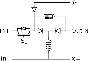
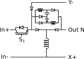
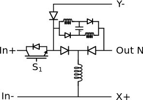
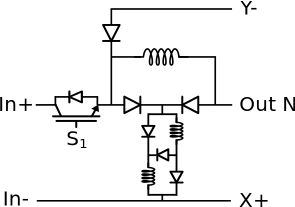
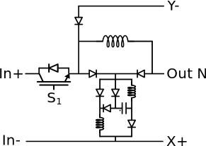
The XY Converter family contains multiple configurations for each of the two parts of the converter. As mentioned, each part operates similarly to a conventional buck-boost. Modifications are based on the modifications of the inductance in the converter part.
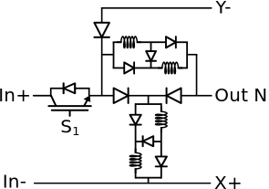
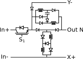
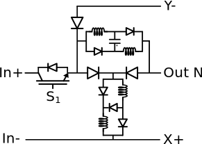
In order to enhance the step-up ability of the converter, it is possible to use one of the configurations shown in Figure 2.
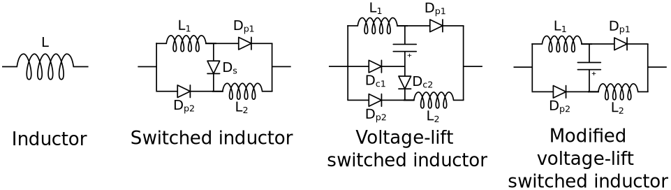
The configuration of the XY Converter can have different effects in operation. For instance, during steady-state operation when the controllable switch is in 'ON' state, diodes Dp1 and Dp2 are conducting for all modifications. This means that inductors are connected in parallel. Thus, equivalent inductance is half the value of a single inductor's inductance. If the Voltage-lift switched inductor is used, the diode Dc1 is conducting, meaning that capacitor is charged by the input voltage source.
Meanwhile, when the switch is in the 'OFF' state, the Dp1 and Dp2 diodes stop conducting. If the switched inductor is used, diode Ds starts conducting, causing the inductors to be in a series connection. On the other hand, using the Voltage-lift switched inductor leads the diode Dc2 to start conducting. This means that inductor current is now discharging the capacitor and the equivalent inductance is twice the inductance of a single inductor.
To sum up, all of the modified inductor configurations allow for 'easier inductor charging' during the 'ON' state of the switch by decreasing the equivalent inductance, while also having 'harder inductor discharging' during the 'OFF' state of the switch (since the equivalent inductance is increased). Naturally, this modification allows for enhanced step-up abilities, which can be further improved by adding one additional capacitor with large capacitance that is charged to the input voltage value. The exact values of input to output voltage ratio of the XY Converter for each of the configurations are given in Table 3.
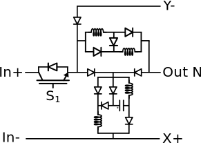
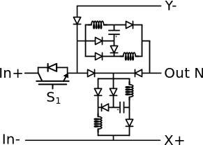
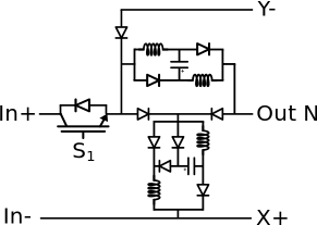
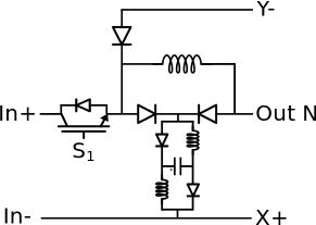
| X part | Y part | Vout/Vin | Configuration Schematic |
|---|---|---|---|
| X inductance type | Y inductance type | Input to output voltage ratio of the converter | Schematic diagram of a configuration |
| Inductor | Inductor |
|
I-I |
| Inductor | Switched inductor |
|
I-SI |
| Inductor | Voltage-lift SI |
|
I-VLSI |
| Inductor | mod. Voltage-lift SI |
|
I-mVLSI |
| Switched inductor | Inductor |
|
SI-I |
| Switched inductor | Switched inductor |
|
SI-SI |
| Switched inductor | Voltage-lift SI |
|
SI-VLSI |
| Switched inductor | mod. Voltage-lift SI |
|
SI-mVLSI |
| Voltage-lift SI | Inductor |
|
VLSI-I |
| Voltage-lift SI | Switched inductor |
|
VLSI-SI |
| Voltage-lift SI | Voltage-lift SI |
|
VLSI-VLSI |
| Voltage-lift SI | mod. Voltage-lift SI |
|
VLSI-mVLSI |
| mod. Voltage-lift SI | Inductor |
|
mVLSI-I |
| mod. Voltage-lift SI | Switched inductor |
|
mVLSI-SI |
| mod. Voltage-lift SI | Voltage-lift SI |
|
mVLSI-VLSI |
| mod. Voltage-lift SI | mod. Voltage-lift SI |
|
mVLSI-mVLSI |
 I-I I-I |
 I-SI I-SI |
 I-VLSI I-VLSI |
 I-mVLSI I-mVLSI |
 SI-I SI-I |
 SI-SI SI-SI |
 SI-VLSI SI-VLSI |
 SI-mVLSI SI-mVLSI |
 VLSI-I VLSI-I |
 VLSI-SI VLSI-SI |
 VLSI-VLSI VLSI-VLSI |
 VLSI-mVLSI VLSI-mVLSI |
 mVLSI-I mVLSI-I |
 mVLSI-SI mVLSI-SI |
 mVLSI-VLSI mVLSI-VLSI |
 mVLSI-mVLSI mVLSI-mVLSI |
Digital Alias
If a converter is controlled by digital inputs, an alias for every digital input used by the converter will be created. Digital input aliases will be available under the Digital inputs list alongside existing Digital input signals. The alias will be shown as Converter_name.Switch_name, where Converter_name is name of the converter component and Switch_name is name of the controllable switch in the converter.
References
- S. B. Mahajan, P. Sanjeevikumar, Patrick Wheeler, Frede Blaabjerg, Marco Rivera, Rishi Kulkarni, 'X-Y Converter Family: A New Breed of Buck Boost Converter for High Step-up Renewable Energy Applications', 2016 IEEE International Conference on Automatica (ICA-ACCA), Oct. 2016.