ANPC Leg
Description of the ANPC Leg component in Schematic Editor
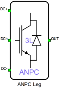
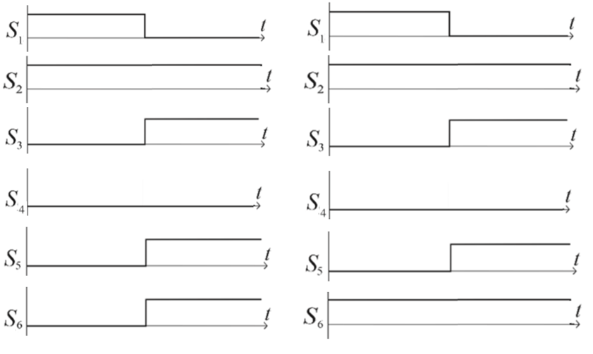
Schematic Block Diagram
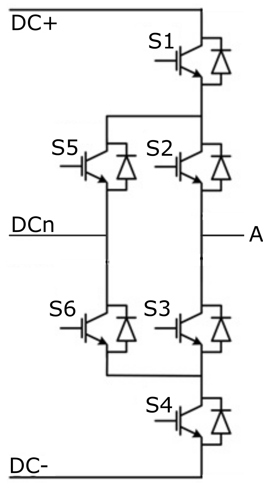
A schematic block diagram of the ANPC Leg component with corresponding switch arrangement and naming is given in Figure 2.
Weight of an ANPC Leg component for real-time simulation is 1.
Control
Selecting Digital inputs as the Control parameter enables assigning gate drive inputs to any of the digital input pins (from 1 to 32(64)). For example, if S1 is assigned to 1, the digital input pin 1 will be routed to the S1 switch gate drive. In addition, the gate_logic parameter selects either active high (High-level input voltage VIH turns on the switch), or active low (Low-level input voltage VIL turns on the switch) gate drive logic, depending on the design of the external controller. In TyphoonSim, digital signals are read from the internal virtual IO bus. Hence, if some signal is sent to digital ouput 1, it will appear on digital input 1.
Selecting Model as the Control parameter, enables setting of the IGBT gate drive signal directly from the signal processing model. The input pin s_ctrl appears on the component. It requires a vector input of six gate drive signals in the following order: [S1, S2, S3, S4, S5, S6]. When controlled from the model, logic is always active high.
PESB Optimization
The PESB Optimization option is available in certain converter models. When PESB Optimization is enabled, all converter's short circuit state space modes will be merged and treated as the same state space mode. For example, if one converter leg within the three phase converter is short circuited and PESB Optimization is enabled, all of the legs within the three phase converter will also be short circuited. This simplification for short circuit modeling can save a significant amount of matrix memory.
Losses calculation
When the Losses calculation property is enabled, the component will calculate switching and conduction power losses for all switching elements (IGBTs and Diodes or MOSFETs). Losses data can be loaded from a standardized xml file, or defined manually by the user. In the case of MOSFET switching elements, the diode characteristic represents the internal MOSFET body diode. When loaded manually, switching power losses are calculated as a function of current, voltage, and temperature using 3D lookup tables. Also, 2D input tables for losses is supported. When a 2D losses table is inserted, it assumes only current and temperature dependence. Conduction power losses can be defined as a function of current and temperature using Vt and Vd lookup tables (LUTs). These LUTs can be 1D or 2D tables. If the LUT is a 1D table, forward voltage drop depends only on the current. If the LUT is a 2D table, the forward voltage drop dependence on the junction temperature is also considered.
In the MOSFET case under reverse current conduction, the current sharing calculation between the MOSFET channel and the internal body diode is performed. Import options and an explanation of how to correctly fill in all the necessary power loss parameters is described in the Importing power losses data section.
All switches are distributed in three groups, and for each group, different power loss parameters can be specified (S1 and S4 are in group 1, S2 and S3 are in group 2, S5 and S6 are in group 3).
In the case of the IGBT switch type in all groups, input/output power losses ports receive/generate vectors of 12 elements (indexes 0-11, where every index in the vector represent one switching element). The ordering of switching elements is described in Table 1.
| Index in the vector | Switching element |
|---|---|
| [0] | S1_igbt |
| [1] | S1_diode |
| [2] | S2_igbt |
| [3] | S2_diode |
| [4] | S3_igbt |
| [5] | S3_diode |
| [6] | S4_igbt |
| [7] | S4_diode |
| [8] | S5_igbt |
| [9] | S5_diode |
| [10] | S6_igbt |
| [11] | S6_diode |
In the case of the MOSFET switch type in all groups, input/output power losses ports receive/generate vectors of 6 elements (indexes 0-5, where every index in the vector represent one switching element). The ordering of switching elements is described in Table 2:
| Index in the vector | Switching element |
|---|---|
| [0] | S1_mosfet |
| [1] | S2_mosfet |
| [2] | S3_mosfet |
| [3] | S4_mosfet |
| [4] | S5_mosfet |
| [5] | S6_mosfet |
If the MOSFET switch type is used for losses group 1 and IGBT switch type for losses groups 2 and 3, input/output power losses ports are vectors of ten elements (every index in the vector represent one switching element). Ordering of switching elements is given in Table 3.
| Index in the vector | Switching element |
|---|---|
| [0] | S1_mosfet |
| [1] | S2_igbt |
| [2] | S2_diode |
| [3] | S3_igbt |
| [4] | S3_diode |
| [5] | S4_mosfet |
| [6] | S5_igbt |
| [7] | S5_diode |
| [8] | S6_igbt |
| [9] | S6_diode |
If the MOSFET switch type is used for losses groups 1 and 2 and the IGBT switch type for losses group 3, input/output power losses ports are vectors of eight elements (every index in the vector represents one switching element). Ordering of switching elements is given in Table 4.
| Index in the vector | Switching element |
|---|---|
| [0] | S1_mosfet |
| [1] | S2_mosfet |
| [2] | S3_mosfet |
| [3] | S4_mosfet |
| [4] | S5_igbt |
| [5] | S5_diode |
| [6] | S6_igbt |
| [7] | S6_diode |
If the MOSFET switch type is used for losses groups 1 and 3 and IGBT switch type for losses group 2, input/output power losses ports are vectors of eight elements (every index in the vector represent one switching element). Ordering of switching elements is given in Table 5.
| Index in the vector | Switching element |
|---|---|
| [0] | S1_mosfet |
| [1] | S2_igbt |
| [2] | S2_diode |
| [3] | S3_igbt |
| [4] | S3_diode |
| [5] | S4_mosfet |
| [6] | S5_mosfet |
| [7] | S6_mosfet |
If the MOSFET switch type is used for losses group 2 and IGBT switch type for losses groups 1 and 3, input/output power losses ports are vectors of ten elements (every index in the vector represent one switching element). Ordering of switching elements is given in Table 6.
| Index in the vector | Switching element |
|---|---|
| [0] | S1_igbt |
| [1] | S1_diode |
| [2] | S2_mosfet |
| [3] | S3_mosfet |
| [4] | S4_igbt |
| [5] | S4_diode |
| [6] | S5_igbt |
| [7] | S5_diode |
| [8] | S6_igbt |
| [9] | S6_diode |
If the MOSFET switch type is used for losses groups 2 and 3 and IGBT switch type for losses group 1, input/output power losses ports are vectors of eight elements (every index in the vector represent one switching element). Ordering of switching elements is given in Table 7.
| Index in the vector | Switching element |
|---|---|
| [0] | S1_igbt |
| [1] | S1_diode |
| [2] | S2_mosfet |
| [3] | S3_mosfet |
| [4] | S4_igbt |
| [5] | S4_diode |
| [6] | S5_mosfet |
| [7] | S6_mosfet |
If the MOSFET switch type is used for losses group 3 and IGBT switch type for losses groups 1 and 2, input/output power losses ports are vectors of ten elements (every index in the vector represent one switching element). Ordering of switching elements is given in Table 8.
| Index in the vector | Switching element |
|---|---|
| [0] | S1_igbt |
| [1] | S1_diode |
| [2] | S2_igbt |
| [3] | S2_diode |
| [4] | S3_igbt |
| [5] | S3_diode |
| [6] | S4_igbt |
| [7] | S4_diode |
| [8] | S5_mosfet |
| [9] | S6_mosfet |
Available component properties are:
-
Losses groups - Switching elements group
- Load Group data from - property to select losses data load source. Available options are User tables and Xml files
- Switch Group type - property to select semiconductor type. Available options are IGBT and MOSFET.
- Current values - Switching elements current axis [A]
-
Voltage values - Switching elements voltage axis [V]
-
Temp values - Switching elements temperature axis [°C]
-
Vt table - Switch forward voltage drop, f(I,T) [V]
-
Vd table - Diode forward voltage drop, f(I,T) [V]
-
Et on table - Switch switching ON losses, output energy, f(I, V, T) [J]
-
Et off table - Switch switching OFF losses, output energy, f(I, V, T) [J]
-
Ed off table - Diode switching OFF losses, output energy, f(I, V, T) [J]
Temperatures calculation
When the Temperatures calculation property is enabled, component will calculate combined power losses (P_loss) and junction temperatures (T_junctions) for all switching elements (IGBTs and diodes). Combined power losses represent sum of the calculated switching and conduction losses transfered through internally generated Thermal network component. The internally generated Thermal network component also calculates junction temperatures from power losses, input case temperatures, and the provided thermal model parameters. Input/output ports for temperatures calculation are vectors of four elements and they are indexed in the same way as explained in the Losses calculation section.
Additional temperature calculation component properties are:
- Thermal networks type - Defines type of internal thermal network
- Rth switch - List of thermal resistance for the IGBT switch
- Tth switch / Cth switch - List of thermal time constants or thermal capacitances for the IGBT switch
- Rth diode - List of thermal resistances for the diode
- Tth diode / Cth diode - List of thermal time constants or thermal capacitances for the diode
- Calculation execution rate - Execution rate in [s] for the losses and temperature calculation logic
Digital Alias
If a converter is controlled by digital inputs, an alias for every digital input used by the converter will be created. Digital input aliases will be available under the Digital inputs list alongside existing Digital input signals. The alias will be shown as Converter_name.Switch_name, where Converter_name is name of the converter component and Switch_name is name of the controllable switch in the converter.
Ports
- DC+ (electrical)
- DC side + port.
- DCn (electrical)
- DC side neutral port.
- DC- (electrical)
- DC side - port.
- OUT (electrical)
- AC side port
- s_crtl (in)
- Available if model control is selected
- Vector of 6 input gate signals for switches
- T_junctions (in)
- Available if Losses calculation is enabled and Temperature calculation is disabled
- Used to provide junction temperatures for switch losses calculations
- If the switch type is IGBT for all switch losses groups, then T_junctions consists of 12 temperature values, one for every switch and diode
- If the switch type is MOSFET for all switch losses groups, then T_junctions consists of 6 temperature values (MOSFET and body diode are having the same temperature)
- T_cases (in)
- Available if Temperature calculation is enabled
- Used to provide case temperatures for the thermal model
- If the switch type is IGBT for all switch losses groups, then T_junctions consists of 12 temperature values, one for every switch and diode
- If the switch type is MOSFET for all switch losses groups, then T_junctions consists of 6 temperature values (MOSFET and the body diode have the same temperature)
- cond_losses (out)
- Available if Losses calculation is enabled
- Represents conduction losses of the switching elements
- If the switch type is IGBT for all switch losses groups, then cond_losses consists of 12 values; If the switch type is MOSFET for all switch losses groups, it consists of 6 values
- sw_losses (out)
- Available if Losses calculation is enabled
- Represents switching losses of the switching elements
- If the switch type is IGBT for all switch losses groups, then sw_losses consists of 12 values; If the switch type is MOSFET for all switch losses groups, it consists of 6 values
- P_loss (out)
- Available if both Losses and Temparature calculation are enabled
- Represents sum of conduction and switching losses of the switching elements
- If the switch type is IGBT for all switch losses groups, then P_loss consists of 12 values; If the switch type is MOSFET for all switch losses groups, it consists of 6 values
- T_junctions (out)
- Available if both Losses and Temparature calculation are enabled. In this case T_junctions is an output since the case thermal model is inside the component and case temperatures are provided as an input to the component.
- Represents the junction temperatures of the switching elements
- If the switch type is IGBT for all switch losses groups, then T_junctions consists of 12 values; If the switch type is MOSFET for all switch losses groups, it consists of 6 values
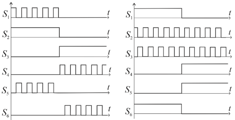
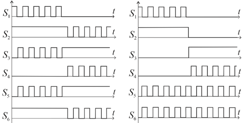
Control (Tab)
- Control
- Specifies how switches are controled. It is possible to choose between: Digital inputs and Model
- More details about each type of control can be found in the Control section
- If Digital inputs is selected as Control, the following properties
can be used:
- S1
- Digital input that is used to control the S1 switch
- S1_logic
- Logic that will be applied to the control signal for S1
- Active high or active low
- S2
- Digital input that is used to control the S2 switch
- S2_logic
- Logic that will be applied to the control signal for S2
- Active high or active low
- S3
- Digital input that is used to control the S3 switch
- S3_logic
- Logic that will be applied to the control signal for S3
- Active high or active low
- S4
- Digital input that is used to control the S4 switch
- S4_logic
- Logic that will be applied to the control signal for S4
- Active high or active low
- S5
- Digital input that is used to control the S5 switch
- S5_logic
- Logic that will be applied to the control signal for S5
- Active high or active low
- S6
- Digital input that is used to control the S6 switch
- S6_logic
- Logic that will be applied to the control signal for S6
- Active high or active low
- Gate control enabling
- If enabled, gives a possibility to control if changes in the gate control signal are applied or not
- Sen
- Available if Gate control enabling is enabled
- Digital input that enables/disables switching
- Sen_logic
- Available if Gate control enabling is enabled
- Logic that will be applied to Sen signal
- S1
- If Model is selected as Control,
the following properties can be used:
- Execution rate
- Defines the period between two updates of gate signals for the component. Gate signals are provided as a signal processing input to component.
- Execution rate
Advanced (Tab)
- PESB Optimization
 PESB Optimization is specific for optimization of real-time simulation and it is not applied to TyphoonSim at all. Changing its value will not affect TyphoonSim simulation at all.
- Enables/disables PESB optimization. More details can be found in the dedicated PESB Optimization section.
- Model Complexity
- Model complexity is specific for optimization of
real-time simulation and it is not applied to TyphoonSim at all. Changing its value
will not affect TyphoonSim simulation.
- Selects model complexity. If 'Optimize resources' is selected, the leg will use less matrix memory in some cases, but the model will be slightly simplified. The simplification is most likely to be visible in passive rectification operation.
Losses (Tab)
- Losses calculation
- Enables/disables losses calculation for converter. More details can be found in the dedicated Losses calculation section.
- Losses groups
- Available if Losses calculation is enabled
- Used to select specific switches group. More details can be found here.
- Load Group data from
- Available if Losses calculation is enabled
- Used to select the source of losses data: user tables or standardized xml files. More information about loading losses data can be found in Import power losses data from XML files
- Switch Group type
- Available if Losses calculation is enabled.
- Specifies switch type: MOSFET or IGBT
- Switch xml file
- Available if Losses calculation is enabled and if Load Group data is set to Xml files
- Used to load losses data for a switch from an xml file. More information about supported file formats can be found in the dedicated section.
- Diode xml file
- Available if Losses calculation is enabled and if Load Group data is set to Xml files
- Used to load losses data for the diode from an xml file. More information about supported file formats can be found in the dedicated section.
- Current values
- Available if Losses calculation is enabled and if Load Group data is set to User tables
- Vector of current values that are used to specify converter losses at specific points
- Up to THCC 2026.1 property would be filled automatically after selecting the xml files
- After THCC 2026.1, if the xml files are in Table only format and are loaded, the property can be set by pressing the Import losses data from xml files
- Voltage values
- Available if Losses calculation is enabled and if Load Group data is set to User tables
- Vector of voltage values that are used to specify converter losses at specific points.
- Up to THCC 2026.1 property would be filled automatically after selecting the xml files
- After THCC 2026.1, if the xml files are in Table only format and are loaded, the property can be set by pressing the Import losses data from xml files
- Temp Values
- Available if Losses calculation is enabled and if Load Group data is set to User tables
- Vector of temperature values that are used to specify converter losses at specific points.
- Up to THCC 2026.1 property would be filled automatically after selecting the xml files
- After THCC 2026.1, if the xml files are in Table only format and are loaded, the property can be set by pressing the Import losses data from xml files
- Vt table
- Available if Losses calculation is enabled and if Load Group data is set to User tables
- 2D look up table for switch conduction voltage drop values.
- Up to THCC 2026.1 property would be filled automatically after selecting the xml files
- After THCC 2026.1, if the xml files are in Table only format and are loaded, the property can be set by pressing the Import losses data from xml files
- More information about table formats can be found in the Losses calculation section.
- Vd table
- Available if Losses calculation is enabled and if Load Group data is set to User tables
- 2D look up table for diode conduction voltage drop values.
- Up to THCC 2026.1 property would be filled automatically after selecting the xml files
- After THCC 2026.1, if the xml files are in Table only format and are loaded, the property can be set by pressing the Import losses data from xml files
- More information about table formats can be found in the Losses calculation section.
- Et on table
- Available if Losses calculation is enabled and if Load Group data is set to User tables
- 3D look up table for switch turn on switching losses.
- Up to THCC 2026.1 property would be filled automatically after selecting the xml files
- After THCC 2026.1, if the xml files are in Table only format and are loaded, the property can be set by pressing the Import losses data from xml files
- More information about table formats can be found in the Losses calculation section.
- Et off table
- Available if Losses calculation is enabled and if Load Group data is set to User tables
- 3D look up table for switch turn off switching losses.
- Up to THCC 2026.1 property would be filled automatically after selecting the xml files
- After THCC 2026.1, if the xml files are in Table only format and are loaded, the property can be set by pressing the Import losses data from xml files
- More information about table formats can be found in the Losses calculation section.
- Ed off table
- Available if Losses calculation is enabled and if Load Group data is set to User tables
- 3D look up table for diode turn off switching losses.
- Up to THCC 2026.1 property would be filled automatically after selecting the xml files
- After THCC 2026.1, if the xml files are in Table only format and are loaded, the property can be set by pressing the Import losses data from xml files
- More information about table formats can be found in the Losses calculation section.
- Import losses data from xml files
- Available if Losses calculation is enabled and if Load Group data is set to User tables
- Pressing the button will set the data from the loaded xml files into the properties for losses current, voltage, temperature, voltage drop and energy tables
- For data to be loaded xml files must be in Table only format
- Temperatures calculation
- Available if Losses calculation is enabled
- Enables/disables losses temperature calculation for converter. Thermal model must be provided. More details can be found in the dedicated Temperatures calculation section.
- Thermal networks type
- Available if Temperature calculation is enabled
- Specifies the type of thermal network model: Foster or Cauer
- Rth switch
- Available if Temperature calculation is enabled
- Switch thermal resistance
- Vector
- Rth diode
- Available if Temperature calculation is enabled
- Diode thermal resistance
- Vector
- Tth switch
- Available if Temperature calculation is enabled and the Thermal network type is Foster
- Switch thermal time constant
- Vector
- Tth diode
- Available if Temperature calculation is enabled and the Thermal network type is Foster
- Diode thermal time constant
- Vector
- Cth switch
- Available if Temperature calculation is enabled and the Thermal network type is Cauer
- Switch thermal capacitance
- Vector
- Cth diode
- Available if Temperature calculation is enabled and the Thermal network type is Cauer
- Diode thermal time constant
- Vector
- Calculations execution rate
- Available if Losses calculation is enabled
- Execution rate for losses calculation. Defines interval that will be used to update losses calculation inputs and outputs.
Extras (Tab)
- Public - Components marked as public expose their signals on all levels.
- Protected - Components marked as protected will hide their signals to components outside of their first locked parent component.
- Inherit - Components marked as inherit will take the nearest parent 'signal_access' property value that is set to a value other than inherit.
References
- Semikron Application Note AN-11001 (link)