Half-bridge Flyback
This reference section describes the properties and features of the Half-bridge Flyback converter component in Schematic Editor
Schematic Block Diagram
A schematic block diagram of the Half-bridge Flyback switching block is given in Figure 1 with its corresponding switch arrangement and naming.
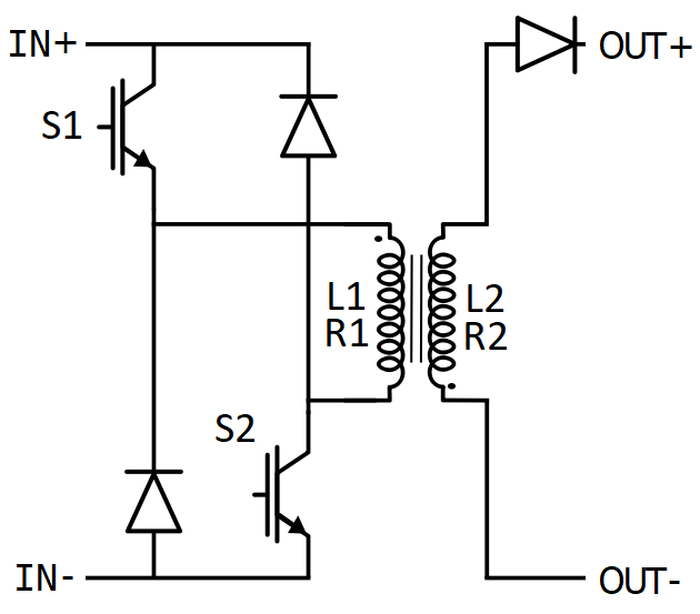
A block diagram and input parameters for the Half-bridge Flyback converter are given in Table 1.
| component | component dialog window | component parameters |
|---|---|---|
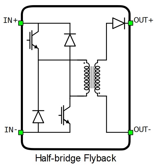 |
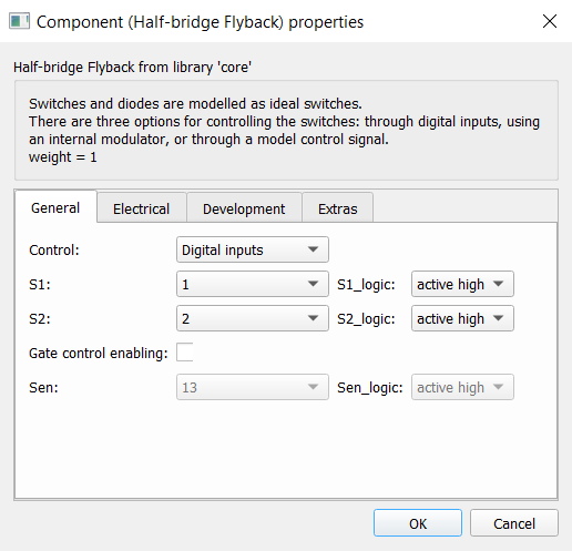 |
|
Control
Digital inputs, when selected as the Control parameter, enables you to assign gate drive inputs to any of the digital input pins (from 1 to 32). For example, if S1 is assigned to 1, the digital input pin 1 will be routed to the S1 switch gate drive. In addition, the S1_logic parameter is set to either active high (i.e. high-level input voltage which turns on the switch) or active low (i.e. low-level input voltage which turns on the switch). The gate drive logic depends on your external controller design. This same behavior also applies to the S2.
The Internal modulator, when selected as the Control parameter, enables you to use the internal PWM modulator for driving the S1 and S2 instead of the digital input pins. In this configuration, three additional component inputs will be present. The En input is used to enable/disable PWM modulator control, In is used as the reference signal input for the first (S1) internal PWM modulator, and In1 is used as the reference signal input for the second (S2) internal PWM modulator.
Model, when selected as the Control parameter, enables you to set the IGBT gate drive signals directly from the signal processing model. The input pin s_ctrl appears on the component. It is a vector input consisting of two signals. The first controls the S1 switch gate, and the second one controls the S2. When controlled from the model, the logic is always set to active high.
The Coupling coefficient parameter applies to the transfer ratio between the coupled inductor currents. During switching transitions, total energy of the inductors remains unchanged for the Coupling coefficient parameter value of 1.
Parameters R1 and R2 are resistance values for parasitic resistors of inductors L1 and L2 respectively. Tuning these resistances can significantly dampen the dynamic transitions during set point changes. Leaving these parameter values at 0 will disable these resistors.
Digital Alias
If a converter is controlled by digital inputs, an alias for every digital input used by the converter will be created. Digital input aliases will be available under the Digital inputs list alongside existing Digital input signals. The alias will be shown as Converter_name.Switch_name, where Converter_name is name of the converter component and Switch_name is name of the controllable switch in the converter.