Diode Leg
Description of the Diode Leg component in Schematic Editor
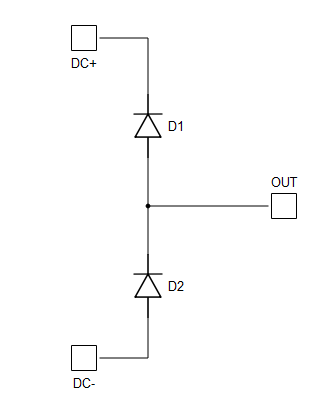
Schematic Block Diagram
A schematic block diagram of the Diode Leg block with corresponding switch arrangement and naming is given in Figure 2.
Weight of a Diode Leg component for real-time/VHIL simulation is 1.
PESB Optimization
The PESB Optimization option is available in certain converter models. When PESB Optimization is enabled, all converter's short circuit state space modes will be merged and treated as the same state space mode. For example, if one converter leg within the three phase converter is short circuited and PESB Optimization is enabled, all of the legs within the three phase converter will also be short circuited. This simplification for short circuit modeling can save a significant amount of matrix memory.
Losses calculation
When the Losses calculation property is enabled, the component will calculate switching and conduction power losses for all switching elements (diodes). Losses data can be loaded from a standardized xml file, or defined manually by the user. Losses data can be loaded from a standardized xml file, or defined manually by the user. When loaded manually, switching power losses are calculated as a function of current, voltage, and temperature using 3D Look-up tables (LUTs). Also, 2D input for losses is supported. When a 2D losses table is inserted, it assumes only current and temperature dependance. Conduction power losses can be defined as a function of current and temperature using Vd Look-up table. These LUTs can be either 1D or 2D. If the LUT is a 1D table, the forward voltage drop depends only on current. If the LUT is a 2D table, the forward voltage drop dependence on the junction temperature is included.
Import options and an explanation of how to correctly fill in all the necessary power loss parameters is described in the Importing power losses data section.
Input/output power losses ports receive/generate vectors of two elements. The first element (index 0) is the upper diode, the second element (index 1) is the bottom diode.
Available mask properties are:
- Current values - Switching elements current axis [A]
- Voltage values - Switching elements voltage axis [V]
- Temp values - Switching elements temperature axis [°C]
- Vd table - Diode forward voltage drop, f(I,T) [V]
- Ed off table - Diode switching OFF losses, output energy, f(I, V, T) [J]
Temperatures calculation
When the Temperatures calculation property is enabled, the component calculates the combined power losses (P_loss) and junction temperatures (T_junctions) for all switching elements (diodes). Combined power losses represent the sum of the calculated switching and conduction losses transferred through an internally generated Thermal network component. The internally generated Thermal network component also calculates the junction temperatures from power losses, input case temperatures, and provided thermal model parameters. Input/output ports for temperature calculation are vectors of two elements and they are indexed in the same way as explained in the Losses calculation section.
Additional temperature calculation mask properties include:
- Thermal networks type - Defines type of internal thermal network
- Diode Rth - List of thermal resistances for diode
- Diode Tth / Cth - List of thermal time constants or thermal capacitances for diode
- Calculation execution rate - Execution rate in [s] for the losses and temperature calculation logic
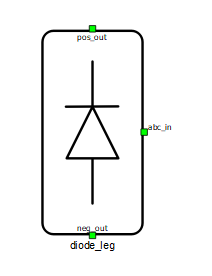
Ports
- pos_out (electrical)
- DC side + port.
- neg_out (electrical)
- DC side - port.
- abc_in (electrical)
- AC side input port
- T_junctions (in)
- Available if Losses calculation is enabled and Temperature calculation is disabled
- Used to provide junction temperatures for switch losses calculations
- T_junctions consists of 2 temperature values, one for every diode
- T_cases (in)
- Available if Temperature calculation is enabled
- Used to provide case temperatures for the thermal model
- T_junctions consists of 2 temperature values, one for every diode
- cond_losses (out)
- Available if Losses calculation is enabled
- Represents conduction losses of the switching elements
- cond_losses consists of 2 values, one for every diode
- sw_losses (out)
- Available if Losses calculation is enabled
- Represents switching losses of the switching elements
- sw_losses consists of 2 values, one for every diode
- P_loss (out)
- Available if both Losses and Temparature calculation are enabled
- Represents sum of conduction and switching losses of the switching elements
- P_loss consists of 2 values, one for every diode
- T_junctions (out)
- Available if both Losses and Temparature calculation are enabled. In this case T_junctions is an output since the case thermal model is inside the component and case temperatures are provided as an input to the component.
- Represents the junction temperatures of the switching elements
- T_junctions consists of 2 values, one for every diode
Advanced (Tab)
- PESB Optimization
 PESB Optimization is specific for optimization of real-time simulation and it is not applied to TyphoonSim at all. Changing its value will not affect TyphoonSim simulation at all.
- Enables/disables PESB optimization. More details can be found in the dedicated PESB Optimization section.
Losses (Tab)
- Losses calculation
- Enables/disables losses calculation for converter. More details can be found in the dedicated Losses calculation section.
- Load data from
- Available if Losses calculation is enabled
- Used to select the source of losses data: user tables or standardized xml files. More information about loading losses data can be found in Import power losses data from XML files
- Diode xml file
- Available if Losses calculation is enabled and if Load data from is set to Xml files
- Used to load losses data for the diode from an xml file. More information about supported file formats can be found in the Losses calculation section.
- Current values
- Available if Losses calculation is enabled and Load data from is set to User tables
- Vector of current values that are used to specify converter losses at specific points.
- Up to THCC 2026.1 property would be filled automatically after selecting the xml files
- After THCC 2026.1, if the xml files are in Table only format and are loaded, the property can be set by pressing the Import losses data from xml files
- Voltage values
- Available if Losses calculation is enabled and Load data from is set to User tables
- Vector of voltage values that are used to specify converter losses at specific points.
- Up to THCC 2026.1 property would be filled automatically after selecting the xml files
- After THCC 2026.1, if the xml files are in Table only format and are loaded, the property can be set by pressing the Import losses data from xml files
- Temp values
- Available if Losses calculation or is enabled and Load data from is set to User tables
- Vector of temperature values that are used to specify converter losses at specific points.
- Up to THCC 2026.1 property would be filled automatically after selecting the xml files
- After THCC 2026.1, if the xml files are in Table only format and are loaded, the property can be set by pressing the Import losses data from xml files
- Vd table
- Available if Losses calculation is enabled and Load data from is set to User tables
- 2D look up table for diode conduction voltage drop values.
- Up to THCC 2026.1 property would be filled automatically after selecting the xml files
- After THCC 2026.1, if the xml files are in Table only format and are loaded, the property can be set by pressing the Import losses data from xml files
- More information about table formats can be found in the Losses calculation section.
- Ed off table
- Available if Losses calculation is enabled and Load data from is set to User tables
- 3D look up table for diode turn off switching losses.
- Up to THCC 2026.1 property would be filled automatically after selecting the xml files
- After THCC 2026.1, if the xml files are in Table only format and are loaded, the property can be set by pressing the Import losses data from xml files
- More information about table formats can be found in the Losses calculation section.
- Import losses data from xml files
- Available if Losses calculation is enabled and if Load data is set to User tables
- Pressing the button will set the data from the loaded xml files into the properties for losses current, voltage, temperature, voltage drop and energy tables
- For data to be loaded xml files must be in Table only format
- Temperatures calculation
- Available if Losses calculation is enabled
- Enables/disables losses temperature calculation for converter. Thermal model must be provided. More details can be found in the dedicated Temperatures calculation section.
- Thermal networks type
- Available if Temperature calculation is enabled
- Specifies the type of thermal network model: Foster or Cauer
- Diode Rth
- Available if Temperature calculation is enabled
- Diode thermal resistance
- Vector
- Diode Tth
- Available if Temperature calculation is enabled and the Thermal network type is Foster
- Diode thermal time constant
- Vector
- Diode Cth
- Available if Temperature calculation is enabled and the Thermal network type is Cauer
- Diode thermal time constant
- Vector
- Calculations execution rate
- Available if Losses calculation is enabled
- Execution rate for losses calculation. Defines interval that will be used to update losses calculation inputs and outputs.
Extras (Tab)
- Public - Components marked as public expose their signals on all levels.
- Protected - Components marked as protected will hide their signals to components outside of their first locked parent component.
- Inherit - Components marked as inherit will take the nearest parent 'signal_access' property value that is set to a value other than inherit.