HERIC
Description of the HERIC converter component in Schematic Editor
Schematic Block Diagrams
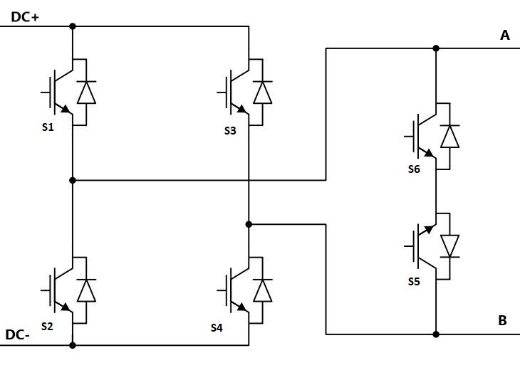
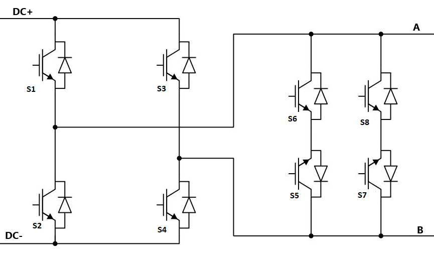
Schematic block diagrams of the single AC clamp HERIC converter and double AC clamp HERIC converter switching block with corresponding switch arrangement and naming are given in Figure 2 and Figure 3, respectively.
Weight of the HERIC converter for real-time/VHIL simulation is 2.
Control
Selecting Digital inputs as the Control parameter enables assigning gate drive inputs to any of the digital input pins (from 1 to 32(64)). For example, if S1 is assigned to 1, the digital input pin 1 will be routed to the S1 switch gate drive. In addition, the gate_logic parameter selects either active high (High-level input voltage VIH turns on the switch), or active low (Low-level input voltage VIL turns on the switch) gate drive logic, depending on the design of the external controller. In TyphoonSim, digital signals are read from the internal virtual IO bus. Hence, if some signal is sent to digital ouput 1, it will appear on digital input 1.
Selecting Model as the Control parameter, enables setting of the IGBTs gate drive signals directly from the signal processing model. The input pin gates appears on the component. It is a six or eight element vector input depending on the AC clamp type. If AC clamp is single, the gate drive signals must be in the following order: [S1, S2, S3, S4, S5, S6]. If AC clamp is double, the gate drive signals must be in the following order: [S1, S2, S3, S4, S5, S6, S7, S8]. When controlled from the model, logic is always active high.
PESB Optimization
The PESB Optimization option is available in certain converter models. When PESB Optimization is enabled, all converter's short circuit state space modes will be merged and treated as the same state space mode. For example, if one converter leg within the three phase converter is short circuited and PESB Optimization is enabled, all of the legs within the three phase converter will also be short circuited. This simplification for short circuit modeling can save a significant amount of matrix memory.
Digital Alias
If a converter is controlled by digital inputs, an alias for every digital input used by the converter will be created. Digital input aliases will be available under the Digital inputs list alongside existing Digital input signals. The alias will be shown as Converter_name.Switch_name, where Converter_name is name of the converter component and Switch_name is name of the controllable switch in the converter.
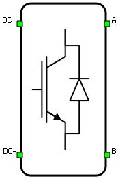
Ports
- DC+ (electrical)
- DC side + port.
- DC- (electrical)
- DC side - port.
- A (electrical)
- AC side port A
- B (electrical)
- AC side port B
- s_ctrl (in)
- Available if model control is selected
- If AC clamp is set to single then s_ctrl is a six element vector input
- If AC clamp is set to double then s_ctrl is an eight element vector input
Control (Tab)
- Control
- Specifies how switches are controlled. It is possible to choose between: Digital inputs and Model
- More details about each type of control can be found in the Control section
- AC clamp
- Specifies the type of AC clamp to be used.
- Available options are: single and double
- If Digital inputs is selected as Control, the following
properties can be used:
- S1
- Digital input that is used to control S1 switch
- S1_logic
- Logic that will be applied to control signal for S1
- Available options are active high or active low
- S2
- Digital input that is used to control S2 switch
- S2_logic
- Logic that will be applied to control signal for S2
- Available options are active high or active low
- S3
- Digital input that is used to control S3 switch
- S3_logic
- Logic that will be applied to control signal for S3
- Available options are active high or active low
- S4
- Digital input that is used to control S4 switch
- S4_logic
- Logic that will be applied to control signal for S4
- Available options are active high or active low
- S5
- Digital input that is used to control S5 switch
- S5_logic
- Logic that will be applied to control signal for S5
- Available options are active high or active low
- S6
- Digital input that is used to control S6 switch
- S6_logic
- Logic that will be applied to control signal for S6
- Available options are active high or active low
- S7
- Available if AC clamp is set to double
- Digital input that is used to control S7 switch
- S7_logic
- Available if AC clamp is set to double
- Logic that will be applied to control signal for S7
- Available options are active high or active low
- S8
- Available if AC clamp is set to double
- Digital input that is used to control S8 switch
- S8_logic
- Available if AC clamp is set to double
- Logic that will be applied to control signal for S8
- Available options are active high or active low
- Gate control enabling
- If enabled, gives a possibility to control if changes in the gate control signal are applied or not
- Sen
- Available if Gate control enabling is enabled
- Digital input that enables/disables switching
- Sen_logic
- Available if Gate control enabling is enabled
- Logic that will be applied to Sen signal
- S1
- If Model is selected as Control, the following properties can be
used:
- Execution rate
- Defines the period between two updates of gate signals for the component. Gate signals are provided as a signal processing input to component
- Execution rate
Advanced (Tab)
- PESB Optimization
 PESB Optimization is specific for optimization of real-time simulation and it is not applied to TyphoonSim at all. Changing its value will not affect TyphoonSim simulation at all.
- Enables/disables PESB optimization. More details can be found in the dedicated PESB Optimization section.
Extras (Tab)
- Public - Components marked as public expose their signals on all levels.
- Protected - Components marked as protected will hide their signals to components outside of their first locked parent component.
- Inherit - Components marked as inherit will take the nearest parent 'signal_access' property value that is set to a value other than inherit.