Zeta Converter
Description of the Zeta Converter component in Schematic Editor
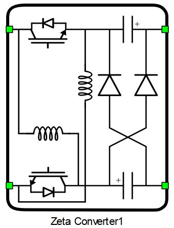
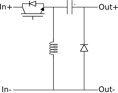
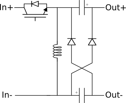
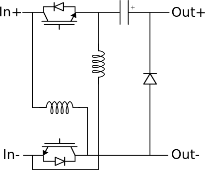
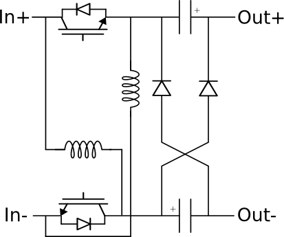
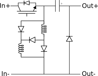
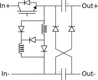
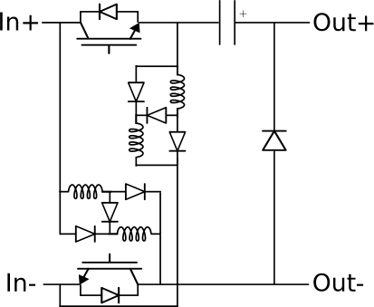
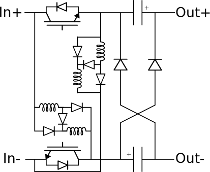
Converter Configurations and Schematic Block Diagram
- Inductor modification: The idea is to use a so-called switched inductor configuration
instead of a single inductor. In steady state operation, when the controllable switch is
in 'ON' state, diodes Dp1 and Dp2 are conducting, meaning that the
inductors L1 and L2 are charged while connected in parallel. When
the controllable switch is in 'OFF' state, only the Ds diode is conducting,
thus connecting these inductors in series during discharge. For this reason, it is
necessary to use the inductors of same value. This means that it is possible to obtain a
larger voltage gain, since the inductance is 'easier to charge and harder to discharge'.
Figure 2. Switched inductor 
- Capacitor modification: Similarly to the switched inductor, it is possible to use two capacitors, here refered to as a 'hybrid-switched capacitor', which further increases the voltage step-up ability of the converter.
- It is possible to use two inductances with corresponding switches. This way, two inductances are charged while in a parallel connection and discharged while in a series connection. The two switches are controlled simultaneously.
| Property value | Vout/Vin | Configuration name | ||
|---|---|---|---|---|
| Inductance type | Double switch/inductor | Use hybrid switched capacitor | Input to output voltage ratio of the converter | Name of the configuration variant that is configured with each set of property values |
| Inductor | False | False |
|
Single inductor |
| Inductor | False | True |
|
Single inductor with hybrid-switched capacitor |
| Inductor | True | False |
|
Double inductor |
| Inductor | True | True |
|
Double inductor with hybrid-switched capacitor |
| Switched inductor | False | False | Switched inductor | |
| Switched inductor | False | True | Switched inductor with hybrid-switched capacitor | |
| Switched inductor | True | False | Double switched inductor | |
| Switched inductor | True | True | Double switched inductor with hybrid-switched capacitor | |
Configurations that utilize a double inductor contain two switches. Since these switches are controlled simultaneously, only one switching signal is used. Therefore, the switch designated as 'S1' in the component parameters can represent one or two controllable switches, depending on how many are included.
Weight of the Zeta Converter component for real-time/VHIL simulation is 2 if Double switch/inductor option is selected, otherwise, weight of the Zeta Converter component for real-time/VHIL simulation is 1.
Control
Selecting Digital inputs as the Control parameter enables assigning gate drive inputs to any of the digital input pins (from 1 to 32(64)). For example, if S1 is assigned to 1, the digital input pin 1 will be routed to the S1 switch gate drive. In addition, the gate_logic parameter selects either active high (High-level input voltage VIH turns on the switch), or active low (Low-level input voltage VIL turns on the switch) gate drive logic, depending on the design of the external controller. In TyphoonSim, digital signals are read from the internal virtual IO bus. Hence, if some signal is sent to digital ouput 1, it will appear on digital input 1.
Selecting Internal modulator as the Control parameter, enables use of the internal PWM modulator for driving S1 switch instead of the digital input pins. In this configuration, two additional component inputs will be present. En input is used to enable/disable the internal PWM modulator, while In is used as a reference signal input.
Selecting Model as the Control parameter, enables setting of the IGBT gate drive signal directly from the signal processing model. The input pin gate appears on the component. It is a 1-element (scalar) input which controls the S1 switch gate. When controlled from the model, logic is always active high.
Digital Alias
If a converter is controlled by digital inputs, an alias for every digital input used by the converter will be created. Digital input aliases will be available under the Digital inputs list alongside existing Digital input signals. The alias will be shown as Converter_name.Switch_name, where Converter_name is name of the converter component and Switch_name is name of the controllable switch in the converter.
Ports
- In+ (electrical)
- DC input + port.
- In- (electrical)
- DC input - port.
- Out+ (electrical)
- DC output + port
- Out- (electrical)
- DC output - port
- s_ctrl (in)
- Available if model control is selected
- 1-element (scalar) input gate signal for switch
- En (in)
- Available if Internal modulator control is selected
- Used to enable/disable internal modulator
- In (in)
- Available if Internal modulator control is selected
- Used to specify modulation signal value for internal modulator
- Freq (in)
- Available if Internal modulator control is selected and Variable carrier frequency is selected as the modulator's operation mode
- Used to specify modulator's carrier frequency
General (Tab)
- Control
- Specifies how switches are controled. It is possible to choose between: Digital inputs, Internal modulator, and Model
- More details about each type of control can be found in the Control section
- If Digital inputs is selected as Control,
the following properties can be used:
- S1
- Digital input that is used to control S1 switch
- S1_logic
- Logic that will be applied to control signal for S1
- Active high or active low
- Gate control enabling
- If enabled, gives a possibility to control if changes in the gate control signal is applied or not
- Sen
- Available if Gate control enabling is enabled
- Digital input that enables/disables switching
- Sen_logic
- Available if Gate control enabling is enabled
- Logic that will be applied to Sen signal
- S1
- If Model is selected as Control,
the following properties can be used:
- Execution rate
- Defines the period between two updates of gate signals for the component. Gate signals are provided as a signal processing input to component.
- Execution rate
- If Internal modulator is selected as Control,
the following properties can be used:
- Operation mode
- Specifies the source of the internal modulator carrier frequency
- If Operation mode is Fixed carrier frequency, then frequency can be specified on the component properties
- If Operation mode is Variable carrier frequency, then the frequency can be specified using a signal processing port
- Carrier frequency (Hz)
- Available if the Operation mode is a Fixed carrier frequency
- Specifies the internal modulator's carrier frequency
- Carrier phase offset
- Specifies the internal modulator's carrier phase offset in degrees
- Dead time period
- Specifies dead time for the internal modulator in seconds
- Reference signal [min, max]
- Specifies carrier signal minimal and maximal value
- Vector containing two values: the minimal carrier signal value, followed by the maximal carrier signal value
- Load mode
- Specifies on which event the new value of the modulation signal will be applied in
the internal modulator
- If on min is selected, new value will be applied when carrier reaches minimal value
- If on max is selected, new value will be applied when carrier reaches maximal value
- If on either is selected, new value will be applied when carrier reaches minimal or maximal value
- Specifies on which event the new value of the modulation signal will be applied in
the internal modulator
- Operation mode
Electrical (Tab)
- Inductance type
- Type of inductor in converter
- Available options are inductor and the switched inductor
- Double switch/inductor
- Enables the use of two equal inductances, each with a corresponding controllable switch. More details in Converter Configurations and Schematic Block Diagram section.
- Inductance
- Inductance of a single inductor [H]
- Initial current
- Inductor initial current [A]
- Hybrid-switched capacitor
- Enables the use of two equal capacitors, along with two diodes instead of one. More details in Converter Configurations and Schematic Block Diagram section.
- Capacitance
- Capacitance of a single capacitor [F]
- Capacitor's ESR
- Specifies equivalent series resistance of a single capacitor [Ω]
- Initial voltage
- Capacitor initial votage [V]
Extras (Tab)
- Public - Components marked as public expose their signals on all levels.
- Protected - Components marked as protected will hide their signals to components outside of their first locked parent component.
- Inherit - Components marked as inherit will take the nearest parent 'signal_access' property value that is set to a value other than inherit.
References
- B. Axelrod, Y. Berkovich and A. Ioinovici, 'Hybrid Switched - Capacitor Ćuk/Zeta/SEPIC Converters in Step-up Mode', 2005 IEEE International Symposium on Circuits and Systems, May 2005.
- M. S. Bhaskar et al., "A New Hybrid Zeta-Boost Converter With Active Quad Switched Inductor for High Voltage Gain," in IEEE Access, vol. 9, pp. 20022-20034, 2021, doi: 10.1109/ACCESS.2021.3054393.