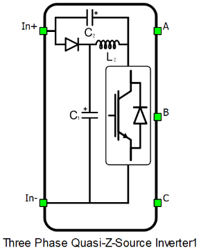
Three Phase Quasi-Z-Source Inverter
Description of the Three Phase Quasi-Z-Source Inverter component in the Schematic Editor Library.
Schematic Block Diagram
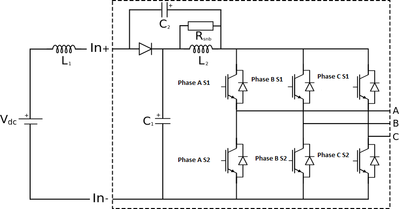
A schematic block diagram of the Three Phase Quasi-Z-Source Inverter switching block is given in Figure 2 with its corresponding switch arrangement and naming.
It should be noted that input inductor L1 should be added externally.
Weight of the Three Phase Quasi-Z-Source Inverter for real-time/VHIL simulation is 3.
Control
Selecting Digital input per switch as the Control parameter enables assigning gate drive inputs to any of the digital input pins (from 1 to 32(64)). For example, if Phase A S1 is assigned to 1, the digital input pin 1 will be routed to the Phase A S1 switch gate drive. In addition, the gate_logic parameter selects either active high (High-level input voltage VIH turns on the switch), or active low (Low-level input voltage VIL turns on the switch) gate drive logic, depending on the external controller design. In TyphoonSim, digital signals are read from the internal virtual IO bus. Hence, if some signal is sent to digital ouput 1, it will appear on digital input 1.
Selecting Model as the Control parameter enables setting the IGBTs' gate drive signals directly from the signal processing model. The input pin gates appears on the component and requires a vector input of six gate drive signals in the following order: [Phase A S1, Phase A S2, Phase B S1, Phase B S2, Phase C S1, Phase C S2]. When controlled from the model, logic is always active high.
Digital Alias
If a converter is controlled by digital inputs, an alias for every digital input used by the converter will be created. Digital input aliases will be available under the Digital inputs list alongside existing Digital input signals. The alias will be shown as Converter_name.Switch_name, where Converter_name is name of the converter component and Switch_name is name of the controllable switch in the converter.
Ports
- In+ (electrical)
- DC side + port.
- In- (electrical)
- DC side - port.
- A (electrical)
- AC side port - phase A.
- B (electrical)
- AC side port - phase B.
- C (electrical)
- AC side port - phase C.
- C1+ (electrical)
- C1 capacitor + port.
- Available if Access to C1 is selected.
- Batt- (electrical)
- C2 capacitor - port.
- Available if Connect external battery is selected.
- Batt+ (electrical)
- C2 capacitor + port.
- Available if Connect external battery is selected.
- s_ctrl
- Available if model control is selected.
- 6-element (vector) input gate signal for switches.
General (Tab)
- Control
- Specifies how switches are controled. It is possible to choose between: Digital input per switch and Model
- More details about each type of control can be found in the Control section
- If Digital input per switch is selected as Control, the following
properties can be used:
- Phase A S1
- Digital input that is used to control Phase A S1 switch
- Phase A S1 logic
- Logic that will be applied to control signal for Phase A S1
- Active high or active low
- Phase A S2
- Digital input that is used to control Phase A S2 switch
- Phase A S2 logic
- Logic that will be applied to control signal for Phase A S2
- Active high or active low
- Phase B S1
- Digital input that is used to control Phase B S1 switch
- Phase B S1 logic
- Logic that will be applied to control signal for Phase B S1
- Active high or active low
- Phase B S2
- Digital input that is used to control Phase B S2 switch
- Phase B S2 logic
- Logic that will be applied to control signal for Phase B S2
- Active high or active low
- Phase C S1
- Digital input that is used to control Phase C S1 switch
- Phase C S1 logic
- Logic that will be applied to control signal for Phase C S1
- Active high or active low
- Phase C S2
- Digital input that is used to control Phase C S2 switch
- Phase C S2 logic
- Logic that will be applied to control signal for Phase C S2
- Active high or active low
- Switching enabled
- If enabled, gives a possibility to control if changes in the gate control signal are applied or not
- Sen
- Available if Gate control enabling is enabled
- Digital input that enables/disables switching
- Sen_logic
- Available if Gate control enabling is enabled
- Logic that will be applied to Sen signal
- Phase A S1
- If Model is selected as Control, the following properties can be
used:
- Execution rate
- Defines the period between two updates of gate signals for the component. Gate signals are provided as a signal processing input to component
- Execution rate
Passive elements (Tab)
- L2 inductance
- Specifies the value of L2 inductance.
- L2 snubber resistor
- Specifies the value of L2 snubber resistor.
- C1 capacitance
- Specifies the value of C1 capacitor.
- C1 ESR
- Specifies the value of C1 equivalent series resistance.
- C2 capacitance
- Specifies the value of C2 capacitor.
- C2 ESR
- Specifies the value of C2 equivalent series resistance.
Measurements (Tab)
-
Phase A S1: I
- Enables internal current measurement for Phase A S1 switch. The signal becomes available in the signals list.
- Phase A S2: I
- Enables internal current measurement for Phase A S2 switch. The signal becomes available in the signals list..
-
Phase B S1: I
- Enables internal current measurement for Phase B S1 switch. The signal becomes available in the signals list.
- Phase B S2: I
- Enables internal current measurement for Phase B S2 switch. The signal becomes available in the signals list.
-
Phase C S1: I
- Enables internal current measurement for Phase C S1 switch. The signal becomes available in the signals list.
- Phase C S2: I
- Enables internal current measurement for Phase C S2 switch. The signal becomes available in the signals list.
- C2: V
- Enables internal voltage measurement for C2 capacitor. The signal becomes available in the signals list..
- Enables internal voltage measurement for C1 capacitor. The signal becomes available in the signals list.
- L1: I
- Enables internal current measurement for L1 inductor. The signal becomes available in the signals list.
Extras (Tab)
- The Extras tab gives you the opportunity to set Signal Access Management for the component.Signal visibility is calculated based on the 'signal_access' property and whether or not a parent component in its hierarchy is locked or not. Components that are not contained within locked components expose their signals regardless of the 'signal_access' property. The 'signal_access' property can have one of three values:
- Public - Components marked as public expose their signals on all levels.
- Protected - Components marked as protected will hide their signals to components outside of their first locked parent component.
- Inherit - Components marked as inherit will take the nearest parent 'signal_access' property value that is set to a value other than inherit.
- Connect External battery
- Selecting this property will enable ports that allow connection of external battery that can be connected in parrallel with C2 capacitor.
- Access to C1
- Selecting this property will enable ports that allow access to C1 capacitor.
References
- J. Anderson and F. Z. Peng, "Four quasi-Z-Source inverters", 2008 IEEE Power Electronics Specialists Conference, Rhodes, 2008, pp. 2743-2749, doi: 10.1109/PESC.2008.4592360.