Bidirectional Cuk
Description of the Cuk converter component in Schematic Editor
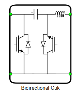
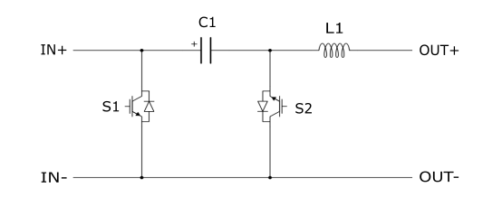
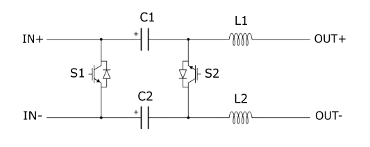
Schematic Block Diagram
A schematic block diagram of the forward switching block is given in Figure 2 and with the Split inductor/capacitor property enabled in Figure 3.
Weight of a Bidirectional Cuk component for real-time/VHIL simulation is 1.
Control
Selecting Digital inputs as the Control parameter enables you to assign gate drive inputs to any of the digital input pins. For example, if S1 is assigned to 1, the digital input pin 1 will be routed to the S1 switch gate drive. In addition, the S1_logic parameter is set to either active high (i.e. high-level input voltage VIH turns on the switch), or active low (i.e. low-level input voltage VIL turns on the switch) gate drive logic, depending on the design of the external controller. In TyphoonSim, digital signals are read from the internal virtual IO bus. Hence, if some signal is sent to digital ouput 1, it will appear on digital input 1.
Selecting Internal modulator as the Control parameter enables you to use the internal PWM modulator for driving the S1 and S2 switches instead of the digital input pins. In this configuration, two additional component inputs will be present. The En input is used to enable/disable PWM modulator control, while In is used as the reference signal input for the internal PWM modulator.
Selecting Model as the Control parameter enables you to set the IGBT gate drive signal directly from the signal processing model. The input pin gate appears on the component. It is a two element input which controls the S1 and S2 switch gate. When controlled from the model, logic is always active high.
Digital Alias
If a converter is controlled by digital inputs, an alias for every digital input used by the converter will be created. Digital input aliases will be available under the Digital inputs list alongside existing Digital input signals. The alias will be shown as Converter_name.Switch_name, where Converter_name is name of the converter component and Switch_name is name of the controllable switch in the converter.
Ports
- IN+ (electrical)
- DC input + port
- IN- (electrical)
- DC input - port
- OUT+ (electrical)
- DC output + port
- OUT- (electrical)
- DC output - port
- gates (in)
- Available if model control is selected
- 2-element (vector) input gate signal for switches
- En (in)
- Available if Internal modulator control is selected
- Used to enable/disable internal modulator
- In (in)
- Available if Internal modulator control is selected
- Used to specify modulation signal value for internal modulator
- Freq (in)
- Available if Internal modulator control is selected and Variable carrier frequency is selected as the modulator's operation mode
- Used to specify modulator's carrier frequency
General (Tab)
- Control
- Specifies how switches are controlled. It is possible to choose between: Digital inputs, Internal modulator, and Model
- More details about each type of control can be found in the Control section
- If Digital inputs is selected as Control, the following
properties can be used:
- S1
- Digital input that is used to control S1 switch
- S1_logic
- Logic that will be applied to control signal for S1
- Active high or active low
- S2
- Digital input that is used to control S2 switch
- S2_logic
- Logic that will be applied to control signal for S2
- Active high or active low
- Gate control enabling
- If enabled, gives a possibility to control if changes in the gate control signal are applied or not
- Sen
- Available if Gate control enabling is enabled
- Digital input that enables/disables switching
- Sen_logic
- Available if Gate control enabling is enabled
- Logic that will be applied to Sen signal
- S1
- If Model is selected as Control, the following properties can
be used:
- Execution rate
- Defines the period between two updates of gate signals for the component. Gate signals are provided as a signal processing input to component
- Execution rate
- If Internal modulator is selected as Control, the following
properties can be used:
- Operation mode
- Specifies the source of the internal modulator carrier frequency
- If Operation mode is Fixed carrier frequency, then the frequency can be specified on the component properties
- If Operation mode is Variable carrier frequency, then the frequency can be specified using a signal processing port
- Carrier frequency (Hz)
- Available if the Operation mode is a Fixed carrier frequency
- Specifies the internal modulator's carrier frequency
- Carrier phase offset
- Specifies the internal modulator's carrier phase offset in degrees.
- Dead time period
- Specifies dead time for the internal modulator in seconds
- Reference signal [min, max]
- Specifies carrier signal minimal and maximal value
- Vector containing two values: the minimal carrier signal value, followed by the maximal carrier signal value
- Load mode
- Specifies on which event the new value of the modulation signal will be
applied in the internal modulator
- If on min is selected, new value will be applied when carrier reaches minimal value
- If on max is selected, new value will be applied when carrier reaches maximal value
- If on either is selected, new value will be applied when carrier reaches minimal or maximal value
- Specifies on which event the new value of the modulation signal will be
applied in the internal modulator
- Operation mode
Electrical (Tab)
- Inductance
- Specifies inductance of the internal inductor
- Initial current
- Specifies initial current of the internal inductor
- Capacitance
- Specifies capacitance of the internal capacitor
- Initial voltage
- Specifies initial voltage of the coupling capacitor
- Capacitor's resistance
- Specifies equivalent series resistance of capacitor
- Split inductor/capacitor
- When the Split inductor/capacitor property is enabled, the converter can be used in an energy bus-based equalization network. All inductances and capacitances are equal
- Figure 3
Measurements (Tab)
- L1: I
- Enables internal current measurement for inductor L1. The signal becomes available in signals list
- C1: V
- Enables internal voltage measurement for capacitor C1. Signal becomes available in signals list
- L2: I
- Enables internal current measurement for inductor L2 when Split inductor/capacitor property is enabled. The signal becomes available in signals list
- C2: V
- Enables internal voltage measurement for capacitor C2 when Split inductor/capacitor property is enabled. Signal becomes available in signals list
Extras (Tab)
- Public - Components marked as public expose their signals on all levels.
- Protected - Components marked as protected will hide their signals to components outside of their first locked parent component.
- Inherit - Components marked as inherit will take the nearest parent 'signal_access' property value that is set to a value other than inherit.