Open Circuit H-Bridge
Description of the Open Circuit H-Bridge component in Schematic Editor
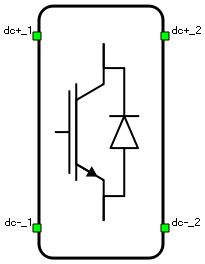
Schematic Block Diagram
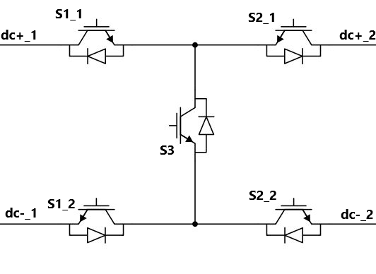
A schematic block diagram of the Open Circuit H-Bridge switching block with corresponding switch arrangement and naming is given in Figure 1.
A block diagram and input parameters for the converter block are given in Table 1.
| component | component dialog window | component parameters |
|---|---|---|
Open Circuit H-Bridge |
 |
|
Control
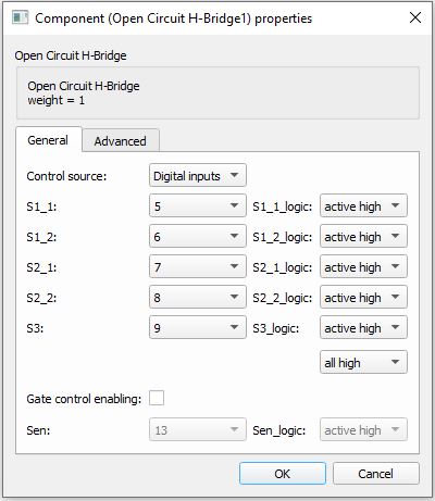
With Digital inputs selected as the Control parameter, enables you to assign gate drive inputs to any of the digital input pins (from 1 to 32(64)). For example, if S1_1 is assigned to 1, the digital input pin 1 will be routed to the S1_1 switch gate drive. In addition, the gate_logic parameter selects either active high (High-level input voltage VIH turns on the switch), or active low (Low-level input voltage VIL turns on the switch) gate drive logic, depending on the user’s external controller design.
If converter is controlled by digital inputs, alias for the every digital input used by converter will be created and it will be available under Digital inputs list alongside with other Digital inputs signals. Alias will be shown as Converter_name.Switch_name, where Converter_name is name of the converter component and Switch_name is name of the controllable switch in the converter.
With Model selected as the Control parameter, enables you to set the IGBTs' gate drive signals directly from signal processing model. The input pin gates appears on the component and requires a vector input of five gate drive signals in the following order: [S1_1, S1_2, S2_1, S2_2, S3]. When controlled from the model, logic is always active high.
PESB Optimization
The PESB Optimization option is available in certain converter models. When PESB Optimization is enabled, all converter's short circuit state space modes will be merged and treated as the same state space mode. For example, if one converter leg within the three phase converter is short circuited and PESB Optimization is enabled, all of the legs within the three phase converter will also be short circuited. This simplification for short circuit modeling can save a significant amount of matrix memory.
Digital Alias
If a converter is controlled by digital inputs, an alias for every digital input used by the converter will be created. Digital input aliases will be available under the Digital inputs list alongside existing Digital input signals. The alias will be shown as Converter_name.Switch_name, where Converter_name is name of the converter component and Switch_name is name of the controllable switch in the converter.