Two Diode Full Wave Rectifier
Description of the Two Diode Full Wave Rectifier component in Schematic Editor
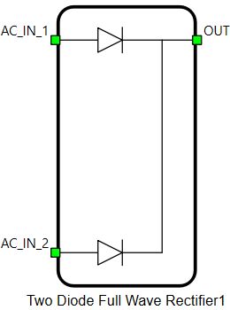
Schematic Block Diagram
A schematic block diagram of the Two Diode Full Wave Rectifier is given in Figure 2.
Weight of a Two Diode Full Wave Rectifier component for real-time/VHIL simulation is 1.
Ports
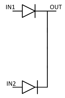
- AC_IN_1 (electrical)
- AC side IN1 port.
- AC_IN_2 (electrical)
- AC side IN2 port.
- OUT (electrical)
- DC side port
General (Tab)
- Reverse diode direction
- Enables reverse diode direction
Extras (Tab)
The Extras tab gives you the opportunity to set Signal Access Management for the component.
Signal visibility is calculated based on the 'signal_access' property and whether or not
a parent component in its hierarchy is locked or not. Components that are not contained
within locked components expose their signals regardless of the 'signal_access'
property. The 'signal_access' property can have one of three values:
- Public - Components marked as public expose their signals on all levels.
- Protected - Components marked as protected will hide their signals to components outside of their first locked parent component.
- Inherit - Components marked as inherit will take the nearest parent 'signal_access' property value that is set to a value other than inherit.
Note: In real-time simulation, the case when both diodes are conducting is not supported by this
model. If both diodes are forward-biased, only one will conduct.