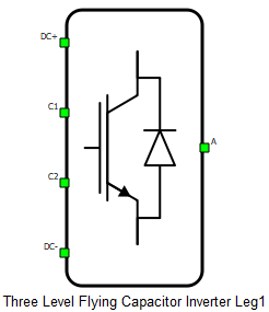
Three Level Flying Capacitor Inverter Leg
Description of the Three Level Flying Capacitor Inverter Leg component in Schematic Editor.
Schematic Block Diagram
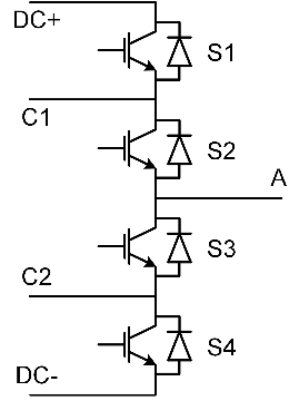
A schematic block diagram of the inverter leg switching block is given in Figure 2 with corresponding switch arrangement and naming.
Weight of Three Level Flying Capacitor Inverter Leg component for real-time simulation is 1.
Control
Digital inputs, when selected as the Control parameter, enables you to assign gate drive inputs to any of the digital input pins (from 1 to 32(64)). For example, if S1 is assigned to 1, the digital input pin 1 will be routed to the S1 switch gate drive. In addition, the S1_logic parameter is set to either active high (i.e. high-level input voltage VIH which turns on the switch), or active low (i.e. low-level input voltage VIL which turns on the switch). The gate drive logic depends on your external controller design. In TyphoonSim, digital signals are read from the internal virtual IO bus. Hence, if some signal is sent to digital ouput 1, it will appear on digital input 1.
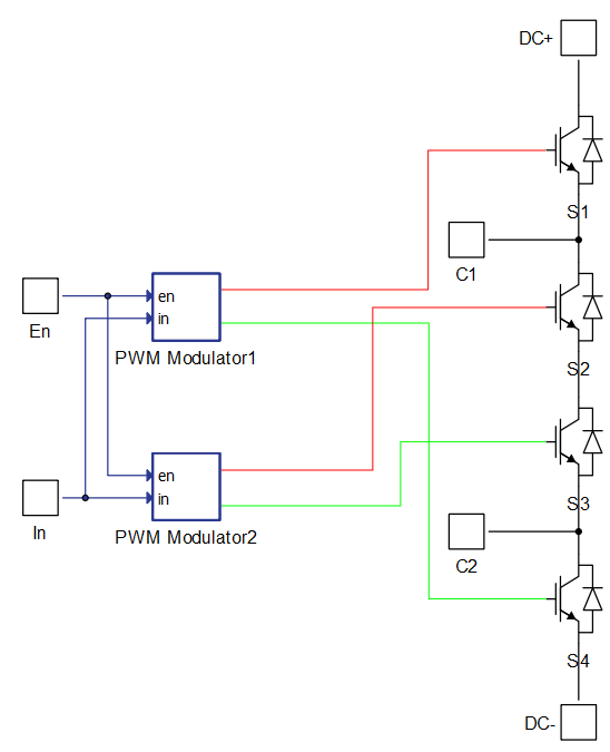
Internal modulator, when selected as the Control parameter, enables you to use the internal PWM modulator for controlling the switches instead of the digital input pins. In this configuration, two additional component inputs appear. The En input is used as enable/disable and In is used as the reference signal input for the internal PWM modulator.
Model, when selected as the Control parameter enables you to set the IGBT's gate drive signal directly from the signal processing model. The input pin gates appears on the component and requires a vector input of four gate drive signals in the following order: [S1, S2, S3, S4]. When controlled from the model, the logic is always set to active high.
Gate control enabling, when checked, enables using an external PWM enabling digital signal.
Figure 3 shows the schematic diagram of the PWM modulation strategy. The PWM Modulator1 uses a triangular carrier with signal range from 0 to 1, while the PWM Modulator2 uses a triangular carrier with signal range from -1 to 0. The red signal is the top output of a modulator, while the green signal is the bottom one.
Timing
When Enable delays is enabled, turn on and turn off delay of the IGBTs will be included in the simulation. More information about this feature can be found on the dedicated switching delay section.
PESB Optimization
The PESB Optimization option is available in certain converter models. When PESB Optimization is enabled, all converter's short circuit state space modes will be merged and treated as the same state space mode. For example, if one converter leg within the three phase converter is short circuited and PESB Optimization is enabled, all of the legs within the three phase converter will also be short circuited. This simplification for short circuit modeling can save a significant amount of matrix memory.
Digital Alias
If a converter is controlled by digital inputs, an alias for every digital input used by the converter will be created. Digital input aliases will be available under the Digital inputs list alongside existing Digital input signals. The alias will be shown as Converter_name.Switch_name, where Converter_name is name of the converter component and Switch_name is name of the controllable switch in the converter.
Ports
- DC+ (electrical)
- DC side + port.
- DC- (electrical)
- DC side - port.
- C1 (electrical)
- DC side flying capacitor port 1.
- C2 (electrical)
- DC side flying capacitor port 2.
- A (electrical)
- AC side port
- s_ctrl (in)
- Available if model control is selected
- Vector of 4 input gate signals for switches
- En (in)
- Available if Internal modulator control is selected
- Used to enable/disable internal modulator
- In (in)
- Available if Internal modulator control is selected
- Used to specify modulation signal value for internal modulator
- Freq (in)
- Available if Internal modulator control is selected and Variable carrier frequency is selected as the modulator's operation mode
- Used to specify modulator's carrier frequency
Control (Tab)
- Control
- Specifies how switches are controled. It is possible to choose between: Digital inputs, Internal modulator, and Model
- More details about each type of control can be found in the Control section
- If Digital inputs is selected as Control, the following
properties can be used:
- S1
- Digital input that is used to control S1 switch
- S1_logic
- Logic that will be applied to control signal for S1
- Active high or active low
- S2
- Digital input that is used to control S2 switch
- S2_logic
- Logic that will be applied to control signal for S2
- Active high or active low
- S3
- Digital input that is used to control S3 switch
- S3_logic
- Logic that will be applied to control signal for S3
- Active high or active low
- S4
- Digital input that is used to control S4 switch
- S4_logic
- Logic that will be applied to control signal for S4
- Active high or active low
- Gate control enabling
- If enabled, gives a possibility to control if changes in the gate control signal are applied or not
- Sen
- Available if Gate control enabling is enabled
- Digital input that enables/disables switching
- Sen_logic
- Available if Gate control enabling is enabled
- Logic that will be applied to Sen signal
- S1
- If Internal modulator is selected as Control, the following
properties can be used:
- Operation mode
- Specifies the source of the internal modulator carrier frequency
- If Operation mode is Fixed carrier frequency, then the frequency can be specified on the component properties
- If Operation mode is Variable carrier frequency, then the frequency can be specified using a signal processing port
- Carrier frequency (Hz)
- Available if the Operation mode is a Fixed carrier frequency
- Specifies the internal modulator's carrier frequency
- Carrier phase offset
- Specifies the internal modulator's carrier phase offset in degrees.
- Dead time
- Specifies dead time for the internal modulator in seconds
- Reference signal [min, max]
- This property is set to [-1.0, 1.0] and cannot be changed
- Specifies carrier signal minimal and maximal value
- Vector containing two values: the minimal carrier signal value, followed by the maximal carrier signal value
- Load mode
- Specifies on which event the new value of the modulation signal will be applied
in the internal modulator
- If on min is selected, new value will be applied when carrier reaches minimal value
- If on max is selected, new value will be applied when carrier reaches maximal value
- If on either is selected, new value will be applied when carrier reaches minimal or maximal value
- Specifies on which event the new value of the modulation signal will be applied
in the internal modulator
- Operation mode
Timing (Tab)
- Enable delays
 Not supported in TyphoonSim yet, hence this signal will be zeroed. Enabling this signal will not affect TyphoonSim simulation at all.
- Enables delays for turn on and off events
- Turn on delay
- Specifies the delay that is applied to turn on events
- Turn off delay
- Specifies the delay that is applied to turn off events
- Vector consisting of current values and corresponding turn off delay. Every current value must be followed by the expected turn off delay.
- Specifies the delay that is applied to turn off events
Advanced (Tab)
- Model type
 Model type options
are not relevant for TyphoonSim simulation and will be ignored.
Model type options
are not relevant for TyphoonSim simulation and will be ignored.- Enables you to choose between two types of models: Reduced and Extended.
- When the Reduced model type is selected, the converter block operates with a reduced number of circuit modes and therefore uses fewer resources. This model type can be used for a typical inverter operation.
- When the Extended model type is selected, the converter block is better suited for rectifier or boost operation, but it will use more resources.
- PESB Optimization
- PESB Optimization is specific for optimization of real-time simulation and it is not applied to TyphoonSim at all. Changing its value will not affect TyphoonSim simulation at all.
- Enables/disables PESB optimization. More details can be found in the dedicated PESB Optimization section.
Extras (Tab)
The Extras tab gives you the opportunity to set Signal Access Management for the component.
- Public - Components marked as public expose their signals on all levels.
- Protected - Components marked as protected will hide their signals to components outside of their first locked parent component.
- Inherit - Components marked as inherit will take the nearest parent 'signal_access' property value that is set to a value other than inherit.