Converters
This section provides a general description of converter components in Typhoon HIL Schematic Editor
In real-time/VHIL simulation, converter switches and diodes are modeled as ideal switches with zero on resistance, infinite off resistance, and instantaneous switching transition (R_on=0, R_off=inf). In addition, for real-time/VHIL simulation, all the converter switching blocks (i.e. Three Phase Inverter, Three Phase Diode Rectifier etc.) are modeled as closed black-boxes that can only be used in the schematic diagram as is. Currently, in real-time/VHIL simulation, it is not possible to construct new switching converters using individual switches (for more context, please refer to this Knowledge Base article). Also, in this simulation context, each power electronics converter has its own weight, as shown in Converter components. The weight of a converter defines how many blocks can be run by a single processing core (SPC). In TyphoonSim, converter weight is not taken into account and can be disregarded.
For simulation in TyphoonSim, converter components are decomposed into single switches components (IGBTs, diodes, or thyristores). Switches and diodes are modeled as changeable resistance (R_on/R_off). In TyphoonSim, it is possible to construct new switching converters by using individual switches.
Converter components
- Diode
- TyphoonSim support - yes
- Weight for real-time/VHIL simulation: 1 - in case ideal switch type is selected, otherwise - /
- MOSFET
- TyphoonSim support - yes
- Weight for real-time/VHIL simulation: 1 - in case ideal switch type is selected, otherwise - /
- Internal modulator support
- IGBT
- TyphoonSim support - yes
- Weight for real-time/VHIL simulation: 1 - in case ideal switch type is selected, otherwise - /
- Internal modulator support
- Thyristor
- TyphoonSim support - yes
- Weight for real-time/VHIL simulation: 1 - in case ideal switch type is selected, otherwise - /
- Buck
- TyphoonSim support - yes
- Weight for real-time/VHIL simulation: 1
- Internal modulator support
- Three Level Buck
- TyphoonSim support - yes
- Weight for real-time/VHIL simulation: 1
- Boost
- TyphoonSim support - yes
- Weight for real-time/VHIL simulation: 1
- Internal modulator support
- Symmetrical Boost
- TyphoonSim support - yes
- Weight for real-time/VHIL simulation: 1
- Internal modulator support
- Quadratic Boost regular
- TyphoonSim support - yes
- Weight for real-time/VHIL simulation: 1
- Internal modulator support
- Quadratic Boost R2P2
- TyphoonSim support - yes
- Weight for real-time/VHIL simulation: 1
- Internal modulator support
- Tapped Inductor Boost
 TyphoonSim support - no
- Weight for real-time/VHIL simulation: 1
- Internal modulator support
- Flying Capacitor Boost
- TyphoonSim support - yes
- Weight for real-time/VHIL simulation: 1 - if additional diodes are not used, 2 - if additional diodes are used
- Internal modulator support
- Buck - Boost
- TyphoonSim support - yes
- Weight for real-time/VHIL simulation: 1
- Internal modulator support
- Tapped Inductor Buck-Boost
- TyphoonSim support - yes
- Weight for real-time/VHIL simulation: 1
- Internal modulator support
- Flyback
- TyphoonSim support - yes
- Weight for real-time/VHIL simulation: 1
- Internal modulator support
- Half-bridge Flyback
- TyphoonSim support - no
- Weight for real-time/VHIL simulation: 1
- Internal modulator support
- Active Clamp Flyback
- TyphoonSim support - yes
- Weight for real-time/VHIL simulation: 1 in case Global GDS oversampling is chosen as Oversampling setting; 2 - in case Switch-level GDS oversampling is chosen as Oversampling setting
- Internal modulator support
- Active Clamp Forward-Flyback (if SPC is selected as Solver
platform)
- TyphoonSim support - yes
- Weight for real-time/VHIL simulation: 2
- Internal modulator support
- Forward
- TyphoonSim support - yes
- Weight for real-time/VHIL simulation: 1
- Internal modulator support
- Active Clamp Forward
- TyphoonSim support - yes
- Weight for real-time/VHIL simulation: 1
- Cuk
- TyphoonSim support - yes
- Weight for real-time/VHIL simulation: 1
- Internal modulator support
- SEPIC
- TyphoonSim support - yes
- Weight for real-time/VHIL simulation: 1
- Internal modulator support
- Bidirectional Cuk
- TyphoonSim support - yes
- Weight for real-time/VHIL simulation: 1
- Internal modulator support
- Push - Pull
- TyphoonSim support - yes
- Weight for real-time/VHIL simulation: 1
- Internal modulator support
- AC Switch
- TyphoonSim support - yes
- Weight for real-time/VHIL simulation: 1
- Diode Leg
- TyphoonSim support - yes
- Weight for real-time/VHIL simulation: 1
- Half Bridge
- TyphoonSim support - yes
- Weight for real-time/VHIL simulation: 1
- Internal modulator support
- Thyristor Leg
- TyphoonSim support - yes
- Weight for real-time/VHIL simulation: 1
- Antiparallel Thyristor Leg
- TyphoonSim support - yes
- Weight for real-time/VHIL simulation: 1
- Three Phase Antiparallel Thyristors
- TyphoonSim support - yes
- Weight for real-time/VHIL simulation: 3
- NPC Leg
- TyphoonSim support - yes
- Weight for real-time/VHIL simulation: 1
- Internal modulator support
- NPC T Type Leg
- TyphoonSim support - yes
- Weight for real-time/VHIL simulation: 1
- Internal modulator support
- ANPC Leg
- TyphoonSim support - yes
- Weight for real-time/VHIL simulation: 1
- MMC Leg - Switching Function
- Three Level Flying Capacitor Inverter Leg
- TyphoonSim support - yes
- Weight for real-time/VHIL simulation: 1
- Internal modulator support
- Four Level Flying Capacitor Inverter Leg
- TyphoonSim support - yes
- Weight for real-time/VHIL simulation: 2
- Five Level Flying Capacitor Inverter Leg
- TyphoonSim support - yes
- Weight for real-time/VHIL simulation: 2
- Seven Level Flying Capacitor Inverter Leg
- TyphoonSim support - yes
- Weight for real-time/VHIL simulation: 3
- ANPC Flying Capacitor Inverter 7 Level Leg
- TyphoonSim support - yes
- Weight for real-time/VHIL simulation: 2
- Nine Level Flying Capacitor Inverter Leg
- TyphoonSim support - yes
- Weight for real-time/VHIL simulation: 4
- ANPC Flying Capacitor Inverter 9 Level Leg
- TyphoonSim support - yes
- Weight for real-time/VHIL simulation: 3
- Single Phase Inverter
- TyphoonSim support - yes
- Weight for real-time/VHIL simulation: 1
- Internal modulator support
- Split-Source Inverter
- TyphoonSim support - no
- Weight for real-time/VHIL simulation: 3
- Internal modulator support
- Single Phase Two Level H5 Inverter
- TyphoonSim support - yes
- Weight for real-time/VHIL simulation: 2
- H6 Single Phase Inverter
- TyphoonSim support - yes
- Weight for real-time/VHIL simulation: 2
- H6_5 Single Phase Inverter
- TyphoonSim support - yes
- Weight for real-time/VHIL simulation: 3
- Three Phase Inverter
- TyphoonSim support - yes
- Weight for real-time/VHIL simulation: 3
- Internal modulator support
- Three Phase NPC Inverter
- TyphoonSim support - yes
- Weight for real-time/VHIL simulation: 3
- Internal modulator support
- Three Phase T Type Inverter
- TyphoonSim support - yes
- Weight for real-time/VHIL simulation: 3
- Internal modulator support
- Three Phase ANPC Inverter
- TyphoonSim support - yes
- Weight for real-time/VHIL simulation: 3
- Three Phase Three Level Flying Capacitor Inverter
- TyphoonSim support - yes
- Weight for real-time/VHIL simulation: 3
- Internal modulator support
- Three Phase Two Level Current Source Inverter
- TyphoonSim support - yes
- Weight for real-time/VHIL simulation: 2
- Three Phase Asymmetric Inverter
- TyphoonSim support - yes
- Weight for real-time/VHIL simulation: 3
- Three Phase Quasi-Z-Source Inverter
- TyphoonSim support - yes
- Weight for real-time/VHIL simulation: 3
- Three Phase Two-Level Current-Source Cycloconverter
- TyphoonSim support - yes
- Weight for real-time/VHIL simulation: 2
- Three Phase Six Pulse Cycloconverter
- TyphoonSim support - yes
- Weight for real-time/VHIL simulation: 3
- Single Phase Diode Rectifier
- TyphoonSim support - yes
- Weight for real-time/VHIL simulation: 1
- Two Diode Full Wave Rectifier
- TyphoonSim support - yes
- Weight for real-time/VHIL simulation: 1
- Active Full Wave Rectifier
- TyphoonSim support - yes
- Weight for real-time/VHIL simulation: 1
- Internal modulator support
- Single Phase Thyristor Rectifier
- TyphoonSim support - yes
- Weight for real-time/VHIL simulation: 2
- Three Phase Diode Rectifier
- TyphoonSim support - yes
- Weight for real-time/VHIL simulation: 3
- Three Phase Thyristor Rectifier
- TyphoonSim support - yes
- Weight for real-time/VHIL simulation: 3
- Vienna Rectifier
- TyphoonSim support - yes
- Weight for real-time/VHIL simulation: 3
- Super Lift Luo
- TyphoonSim support - yes
- Weight for real-time/VHIL simulation: 1
- Internal modulator support
- HERIC
- TyphoonSim support - yes
- Weight for real-time/VHIL simulation: 2
- XY Converter
- TyphoonSim support - no
- Weight for real-time/VHIL simulation: 2
- Internal modulator support
- Zeta Converter
- TyphoonSim support - yes
- Weight for real-time/VHIL simulation: 1 - in case single switch/inductor is used, 2 - in case double switch/inductor is used
- Internal modulator support
- 5L NE Type Converter
- TyphoonSim support - yes
- Weight for real-time/VHIL simulation: 2
- Phase Shifted Full Bridge Converter
- TyphoonSim support - yes
- Weight for real-time/VHIL simulation: 3
- Internal modulator support
Each SPC has processing capability for power electronics switching blocks weighing 3 or 4, depending on the device used and its configuration. Let's assume that maximum available converter weight per SPC is 3 on the chosen device configuration. For example, a Buck converter weighs 1 and a 5L NE Type converter weighs 2, so these two PESBs can fit together in one SPC. Three Buck converters can also fit into one SPC. A Three Phase Inverter weighs 3, so an additional converter cannot fit into the same SPC as this inverter. Just as a reminder, circuits are split into separate processing cores using some of the available coupling components.
Enhanced Resolution converters
Enhanced Resolution converters are converters that do not use FPGA resources that are typically utilized by converters, i.e., they are not simulated using SPC-owned resources. Instead, these converters are run on a specialized FPGA hardware resource that is optimized for certain converter topology group in order to reduce the simulation time step. These specialized resources are present in some HIL device configurations (see Device Configuration Table). More details about a specific converter solver can be found in the dedicated document for that given solver.
In TyphoonSim, Enhanced Resolution converters are implemented in the same manner as all other converter library components, as it is explained in the section above.
At the moment, the following specialized converter solvers are available:
The current version of Schematic Editor offers a selection of the following types of enhanced resolution converter components:
- Dual Active Bridge
- TyphoonSim support - yes
- Internal modulator support
- Resonant Converter
- TyphoonSim support - yes
- Internal modulator support
- Active Clamp Forward-Flyback (if UltraCore is selected as
Solver platform)
- TyphoonSim support - yes
- Internal modulator support
Converter control options
- Digital inputs (per switch or per leg) - per switch is supported by all controllable converters
- Internal modulator (internal FPGA-based modulator) - supported by a subset of converters listed in Converter components
- Model (direct switch control from the signal processing model) - supported by all controllable converters, except for the enhanced resolution ones
Digital inputs control options are supported by all controllable converters by default. GDS oversampling time (for example: the PWM gate drive signal) is higher than the simulation time step, which is as high as 6.25 ns for HIL402, 602+, and 604 devices, 4.5 ns for HIL101 devices, and 3.5 ns for HIL404, HIL506, and HIL606 devices. In TyphoonSim, digital signals are read from the internal virtual IO bus. Hence, if some signal is sent to digital ouput 1, it will appear on digital input 1.
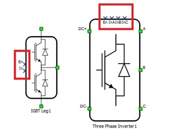
When Internal modulator is selected as control option, there is one Enable input and 1 to 3 reference signal inputs depending on the number of PWM channels used. For example, Half Bridge uses 1 PWM channel which requires only 1 reference input. Three Phase Inverter requires 3 PWM channels and 3 corresponding reference inputs. Figure 1 shows the PWM modulator inputs for the Half Bridge and Three Phase Inverter components.
If the control option is set to Model, an additional signal input will appear: the input vector for the gate drive signals. The length of the input vector is equal to the number of controllable switches in the converter. For example, Half Bridge has 2 controllable switches, so control signal length is 2, while Three Phase Inverter has 6 controllable switches, so control signal length is 6.
PWM enabling
PWM signals are activated by checking the PWM enabling checkbox ender the General tab in converter components.
The Sen parameter selects the digital input pin to supply the external PWM enabling signal. When the signal is active, PWM signals are enabled and control corresponding converter switches. The Sen_logic parameter selects either active high (High-level on the digital input turns on the PWM signals) or active low (Low-level on the digital input turns on the PWM signals) digital logic.
Timing
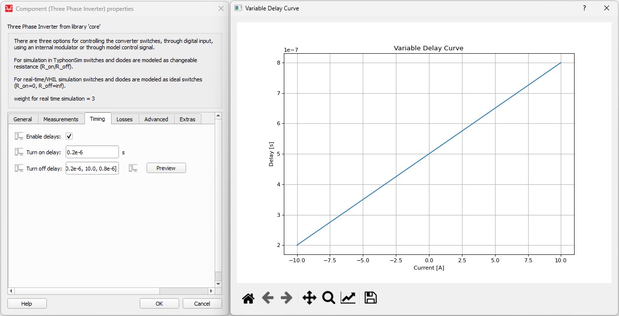
Switching delay - Timing feature models turn on and off delays for IGBTs (delay from active gate signal transition to the start of conducting and vice versa). The Turn Off switching delay option is defined as a function of the output current at the moment of switching, while the Turn On Delay option is constant. The maximum value of the delay is limited to 10 µs.
Since the Switching Delay block is placed before the DTV (Dead Time Violation) logic, it can also be used to detect the minimum dead time period duration. In that case, Turn On Delay should be set to zero and Turn Off Delay should be set to the minimum dead time duration value.
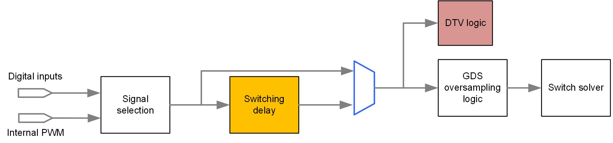
Switching delay is activated by checking the Enable delays checkbox under the Timing tab in converter components. Fixed and variable delays can be defined. Turn Off variable delay can be defined in vector form, as shown in Figure 3.
Measurements
It is possible to enable internal current measurements of the switches inside a power electronics switching block. The specific currents to be measured can be chosen by checking the box next to their name.
Checked measurement will appear in the list of output variables as Converter name.Switch name_I. For example, if the converter name is Half Bridge and the current measurement of Half Bridge S2 (bottom) switch is checked, an analog signal named Half Bridge.S2_I will appear in analog output variables list.
PESB Optimization
The PESB Optimization option is available in certain converter models. When PESB Optimization is enabled, all converter's short circuit state space modes will be merged and treated as the same state space mode. For example, if one converter leg within the three phase converter is short circuited and PESB Optimization is enabled, all of the legs within the three phase converter will also be short circuited. This simplification for short circuit modeling can save a significant amount of matrix memory.
Digital Alias
If a converter is controlled by digital inputs, an alias for every digital input used by the converter will be created. Digital input aliases will be available under the Digital inputs list alongside existing Digital input signals. The alias will be shown as Converter_name.Switch_name, where Converter_name is name of the converter component and Switch_name is name of the controllable switch in the converter.