Switch-level GDS oversampling
Overview and description of the Switch-level GDS oversampling feature in Typhoon HIL Control Center. Switch-level GDS oversampling is designed to compensate all GDS transitions within one simulation step, in contrast to global GDS oversampling.
Switch-level GDS oversampling overview
Switch-level GDS oversampling is implemented at component level. Check Table 1 to see which components support Switch-level GDS oversampling. While most models works well with Global GDS oversampling, those models which have a high switching frequency and where more than one GDS transition can happen during one simulation step should be simulated using Switch-level GDS oversampling. Typical examples are Dual-Active-Bridge and Resonant converter applications.
| Converters that supports Switch-level GDS oversampling | |
|---|---|
| Converter name | Weight |
| Half Bridge | 1 |
| Boost | 1 |
| Active Clamp Forward-Flyback | 2 |
| Active Clamp Flyback | 1 - in case Global GDS oversampling is chosen as Oversampling setting; 2 - in case Switch-level GDS oversampling is chosen as Oversampling setting |
The working principle of Switch-level GDS oversampling is explained using a Half Bridge example. As mentioned earlier, Switch-level GDS oversampling is designed to compensate all GDS transitions within one simulation step. This is done in the following way:
- Average duty cycle for every controllable switch is calculated at the simulation step level. Because of that, all transitions will be compensated. In Figure 1 you can see two gate drive signals whose values are changed during one simulation step. Also, you can see how the average duty cycle changes for both signals. These average duty cycle values are fed into the converter. The duty cycle will be calculated very precisely thanks to a small GDS sampling period. Check GDS oversampling for more details.
- The converter receives information about duty cycles of the gate drive signals, and then this information is used to calculate the converter’s output. The converter is modelled using controlled voltage and current sources. Figure 2 shows the model of a Half Bridge component which uses Switch-Level GDS oversampling. Voltage and current sources are controlled by average GDS duty cycles. Since averaging is done at the simulation step level and the simulation step period is small in comparison to the PWM period, the switching ripple will be preserved. Since diodes are present in the model, the component supports discontinuous conduction mode.
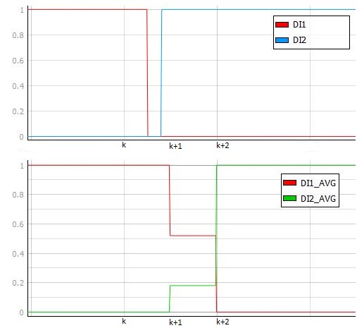
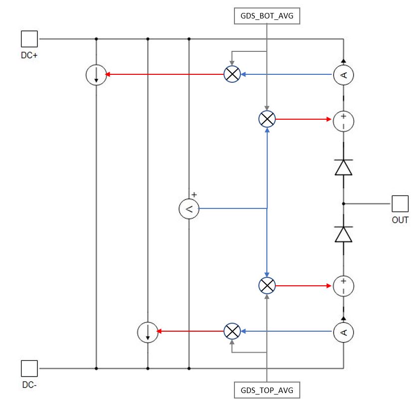
Figure 3 shows a model that includes a Half Bridge that uses Switch-level GDS oversampling, while Figure 4 shows a comparison of results observed from this model with the reference results that are observed with the offline solver. You can see that a difference occurs in the moments when the GDS is changed, but it is obvious that the converter successfully compensates an error that would be present due to sampling error in the case when Switch-level GDS oversampling is not used. Also, it is important to mention that due to algorithm complexity, Switch-level GDS oversampling introduces a delay of one simulation step between the GDS inputs and the states outputs. That can be observed from the results, as it is obvious that L_SL_gds_ovs is delayed by one simulation step relative to L_reference.
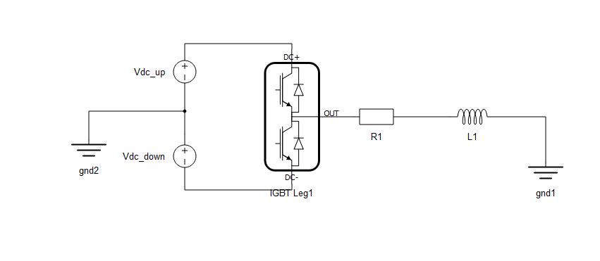
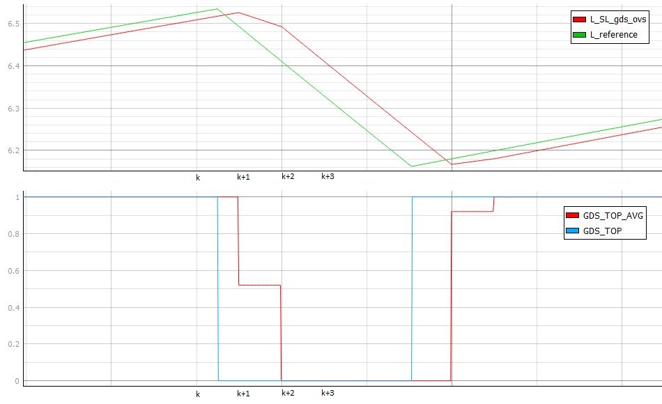
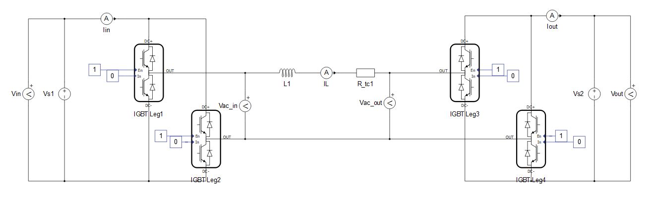
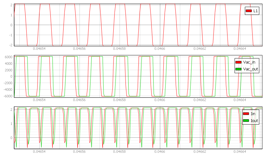
Figure 5 shows a model of the Dual-Active-Bridge converter. The switching frequency is set to 80 kHz, while the simulation step is set to 0.5 microseconds. This model is simulated using the Switch-level GDS oversampling feature. Figure 6 shows results observed from the simulation. As you can see, observed results are as expected and all waveforms have their expected shapes. So, it is possible to precisely simulate a DAB converter if Switch-level GDS oversampling is used, even in the case when the switching frequency is relatively large.
GDS Oversampling frequency and minimum timestep
The GDS Oversampling resolution is defined by the IO timing of the device. More information is available in the IO Timing section of each HIL Simulator device's documentation. This means it can be as high as 6.25 ns for HIL402, 602+, and 604 devices, 4.5 ns for HIL101 devices, and 3.5 ns for HIL404, HIL506, and HIL606 devices.