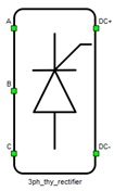
Three Phase Thyristor Rectifier
Description of the Three Phase Thyristor Rectifier component in Schematic Editor
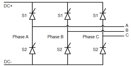
Schematic Block Diagram
A schematic block diagram of a three-phase thyristor rectifier block is given in Figure 2.
Weight of Three Phase Thyristor Rectifier component for real-time simulation is 3.
Control
Selecting Digital inputs as the Control parameter, enables assigning gate drive inputs to any of the digital input pins (from 1 to 32 (64)). For example, if Phase A S1 is assigned to 1, the digital input pin 1 is routed to the Phase A S1 switch gate drive. In addition, the gate_logic parameter selects either active high (High-level input voltage VIH turns on the switch), or active low (Low-level input voltage VIL turns on the switch) gate drive logic, depending on the external controller design. In TyphoonSim, digital signals are read from the internal virtual IO bus. Hence, if some signal is sent to digital ouput 1, it will appear on digital input 1.
Selecting Model as the Control parameter enables setting the thyristor gate drive signals directly from signal processing model. The input pin that appear on the top of the rectifier requires a vector input of six gate drive signals in the following order: [Phase A S1, Phase A S2, Phase B S1, Phase B S2, Phase C S1, Phase C S2]. When controlled from the model, logic is always active high.
PESB Optimization
The PESB Optimization option is available in certain converter models. When PESB Optimization is enabled, all converter's short circuit state space modes will be merged and treated as the same state space mode. For example, if one converter leg within the three phase converter is short circuited and PESB Optimization is enabled, all of the legs within the three phase converter will also be short circuited. This simplification for short circuit modeling can save a significant amount of matrix memory.
Losses calculation
When the Losses calculation property is enabled, the component will calculate switching and conduction power losses for all switching elements (Thyristors). Switching power losses are calculated as a function of current, voltage, and temperature using 3D Look-up tables (LUTs). Also, 2D input for losses is supported. When a 2D losses table is inserted, it assumes only current and temperature dependance. Conduction power losses can be defined as a function of current and temperature using Vt Look-up tables. These LUTs can be either 1D or 2D. If the LUT is a 1D table, the forward voltage drop depends only on current. If the LUT is a 2D table, the forward voltage drop dependence on the junction temperature is included.
Input/output power losses ports receive/generate vectors of six elements. The first element (index 0) is the upper thyristor in phase A, the second element (index 1) is the bottom thyristor in phase A. The next two elements are the phase B upper and bottom thyristor, respectively. The 4th and 5th elements follow this same pattern for phase C.
Available mask properties are:
- Current values - Switching elements current axis [A]
- Voltage values - Switching elements voltage axis [V]
- Temp values - Switching elements temperature axis [°C]
- Vt table - Thyristor forward voltage drop, f(I,T) [V]
- Et on table - Thyristor switching ON losses, output energy, f(I, V, T) [J]
Temperatures calculation
When the Temperatures calculation property is enabled, the component calculates the combined power losses (P_loss) and junction temperatures (T_junctions) for all switching elements (Thyristors). Combined power losses represent the sum of the calculated switching and conduction losses transferred through an internally generated Thermal network component. The internally generated Thermal network component also calculates the junction temperatures from power losses, input case temperatures, and provided thermal model parameters. Input/output ports for temperatures calculation are vectors of six elements and they are indexed in the same way as explained in the Losses calculation section.
Additional temperature calculation mask properties include:
- Thermal networks type - Defines type of internal thermal network
- Thyristor Rth - List of thermal resistances for thyristor
- Thyristor Tth / Cth- List of thermal time constants or thermal capacitances for thyristor
- Calculation execution rate - Execution rate in [s] for the losses and temperature calculation logic
Digital Alias
If a converter is controlled by digital inputs, an alias for every digital input used by the converter will be created. Digital input aliases will be available under the Digital inputs list alongside existing Digital input signals. The alias will be shown as Converter_name.Switch_name, where Converter_name is name of the converter component and Switch_name is name of the controllable switch in the converter.
Ports
- DC+ (electrical)
- DC side + port.
- DC- (electrical)
- DC side - port.
- A (electrical)
- AC side port - phase A
- B (electrical)
- AC side port - phase B
- C (electrical)
- AC side port - phase C
- gates (in)
- Available if model control is selected
- Vector of 6 input gate signals for switches
- T_junctions (in)
- Available if Losses calculation is enabled and Temperature calculation is disabled
- Used to provide junction temperatures for switch losses calculations
- T_junctions consists of 6 temperature values, one for every thyristor
- T_cases (in)
- Available if both Losses and Temparature calculation are enabled
- Used to provide case temperatures for the thermal model
- T_cases consists of 6 temperature values, one for every thyristor
- cond_losses (out)
- Available if Losses calculation is enabled and Temperature calculation is disabled
- Represents conduction losses of the switching elements
- cond_losses consists of 6 values
- sw_losses (out)
- Available if Losses calculation is enabled and Temperature calculation is disabled
- Represents switching losses of the switching elements
- sw_losses consists of 6 values
- P_loss (out)
- Available if both Losses and Temparature calculation are enabled
- Represents sum of conduction and switching losses of the switching elements
- P_loss consists of 6 values
- T_junctions (out)
- Available if both Losses and Temparature calculation are enabled. In this case T_junctions is an output since the case thermal model is inside the component and case temperatures are provided as an input to the component.
- Represents the junction temperatures of the switching elements
- T_junctions consists of 6 values
General (Tab)
- Control
- Specifies how switches are controled. It is possible to choose between: Digital inputs and Model
- More details about each type of control can be found in the Control section
- If Digital inputs is selected as Control, the following
properties can be used:
- Phase A S1
- Digital input that is used to control phase A S1 switch
- Phase A S1 logic
- Logic that will be applied to control signal for phase A S1
- Active high or active low
- Phase A S2
- Digital input that is used to control phase A S2 switch
- Phase A S2 logic
- Logic that will be applied to control signal for phase A S2
- Active high or active low
- Phase B S1
- Digital input that is used to control phase B S1 switch
- Phase B S1 logic
- Logic that will be applied to control signal for phase B S1
- Active high or active low
- Phase B S2
- Digital input that is used to control Phase B S2 switch
- Phase B S2 logic
- Logic that will be applied to control signal for phase B S2
- Active high or active low
- Phase C S1
- Digital input that is used to control phase C S1 switch
- Phase C S1 logic
- Logic that will be applied to control signal for phase C S1
- Active high or active low
- Phase C S2
- Digital input that is used to control Phase C S2 switch
- Phase C S2 logic
- Logic that will be applied to control signal for phase C S2
- Active high or active low
- Gate control enabling
- If enabled, gives a possibility to control if changes in the gate control signal are applied or not
- Sen
- Available if Gate control enabling is enabled
- Digital input that enables/disables switching
- Sen_logic
- Available if Gate control enabling is enabled
- Logic that will be applied to Sen signal
- Phase A S1
- If Model is selected as Control, the following properties can be
used:
- Execution rate
- Defines the period between two updates of gate signals for the component. Gate signals are provided as a signal processing input to component
- Execution rate
Measurements (Tab)
- Phase A S1: I
 Not supported in TyphoonSim yet, hence this signal will be zeroed. Enabling this signal will not affect TyphoonSim simulation at all.
- Enables internal current measurement for switch S1 in Phase A. The signal becomes available in the signals list.
- Phase A S2: I
-
Not supported in TyphoonSim yet, hence this signal will be zeroed. Enabling this signal will not
affect TyphoonSim simulation at all.
- Enables internal current measurement for switch S2 in Phase A. The signal becomes available in the signals list.
-
Phase B S1: I
-
Not supported in TyphoonSim yet, hence this signal will be zeroed. Enabling this signal will not
affect TyphoonSim simulation at all.
- Enables internal current measurement for switch S1 in Phase B. The signal becomes available in the signals list.
- Phase B S2: I
-
Not supported in TyphoonSim yet, hence this signal will be zeroed. Enabling this signal will not
affect TyphoonSim simulation at all.
- Enables internal current measurement for switch S2 in Phase B. The signal becomes available in the signals list.
- Phase C S1: I
-
Not supported in TyphoonSim yet, hence this signal will be zeroed. Enabling this signal will not
affect TyphoonSim simulation at all.
- Enables internal current measurement for switch S1 in Phase C. The signal becomes available in the signals list.
- Phase C S2: I
-
Not supported in TyphoonSim yet, hence this signal will be zeroed. Enabling this signal will not
affect TyphoonSim simulation at all.
- Enables internal current measurement for switch S2 in Phase C. The signal becomes available in the signals list.
Advanced (Tab)
-
PESB Optimization is specific for optimization of real-time simulation and it is not applied to TyphoonSim at all. Changing its value will not affect TyphoonSim simulation at all.
- Enables/disables PESB optimization. More details can be found in the dedicated PESB Optimization section.
Losses (Tab)
- Losses calculation
- Enables/disables losses calculation for converter. More details can be found in the dedicated Losses calculation section.
- Current values
- Available if Losses calculation is enabled
- Vector of current values that are used to specify converter losses at specific points.
- Voltage values
- Available if Losses calculation is enabled
- Vector of voltage values that are used to specify converter losses at specific points.
- Temp Values
- Available if Losses calculation is enabled
- Vector of temperature values that are used to specify converter losses at specific points.
- Vt table
- Available if Losses calculation is enabled
- 2D look up table for switch conduction voltage drop values. More information about table formats can be found in the Losses calculation section.
- Et on table
- Available if Losses calculation is enabled
- 3D look up table for switch turn on switching losses. More information about table formats can be found in the Losses calculation section.
- Temperatures calculation
- Available if Losses calculation is enabled
- Enables/disables losses temperature calculation for converter. Thermal model must be provided. More details can be found in the dedicated Temperatures calculation section.
- Thermal networks type
- Available if Temperature calculation is enabled
- Specifies the type of thermal network model: Foster or Cauer
- Thyristor Rth
- Available if Temperature calculation is enabled
- Thyristor thermal resistance
- Vector
- Thyristor Tth
- Available if Temperature calculation is enabled and the Thermal network type is Foster
- Thyristor thermal time constant
- Vector
- Thyristor Cth
- Available if Temperature calculation is enabled and the Thermal network type is Cauer
- Thyristor thermal capacitance
- Vector
- Calculations execution rate
- Available if Losses calculation is enabled
- Execution rate for losses calculation. Defines interval that will be used to update losses calculation inputs and outputs.
Extras (Tab)
- Public - Components marked as public expose their signals on all levels.
- Protected - Components marked as protected will hide their signals to components outside of their first locked parent component.
- Inherit - Components marked as inherit will take the nearest parent 'signal_access' property value that is set to a value other than inherit.