Three Phase NPC Inverter
Description of the Three Phase NPC Inverter component in Schematic Editor
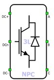
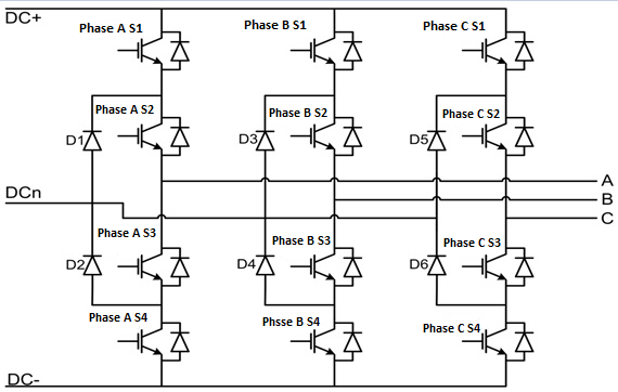
Schematic Block Diagram
A schematic block diagram of the inverter switching block is given in Figure 2 with corresponding switch arrangement and naming.
Weight of a Three Phase NPC Inverter component for real-time/VHIL simulation is 3.
Control
Digital input per switch, when selected as the Control parameter, enables you to assign gate drive inputs to any of the digital input pins (from 1 to 32). For example, if Phase A S1 is assigned to 1, the digital input pin 1 will be routed to the Phase A S1 switch gate drive. In addition, the gate_logic parameter selects either active high (i.e. high-level input voltage VIH turns on the switch), or active low (i.e. low-level input voltage VIL turns on the switch) gate drive logic, depending on your external controller design.
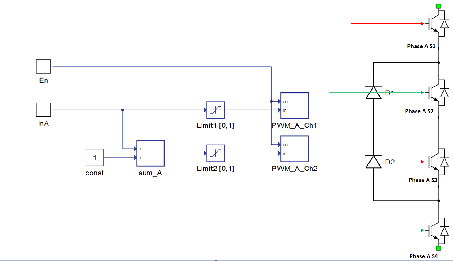
Internal modulator, when selected as the Control parameter, enables you to use internal PWM modulator for driving the converter's switches instead of digital input pins. In this configuration, four additional component inputs will be present. En input is used to enable/disable PWM modulator control, while InA, InB, and InC are used as referent signal inputs for the internal PWM modulator. Overall, 6 PWM channels are used to drive the three level three phase NPC converter, 2 per phase. Reference signals for 2 modulators that control the switches of a single phase leg, are created from a single reference input. A block diagram of one phase leg controlled by PWM modulators is shown in Figure 3. The input reference signal is in range from -1.0 to 1.0. This signal is split into two reference signals for two modulators, and set to a range from 0.0 to 1.0.
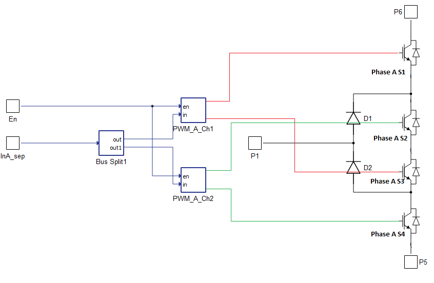
Internal modulator separated, when selected as the Control parameter, enables you to use the internal PWM modulator for driving the converter's switches instead of digital input pins. Additional component inputs and the number of created internal PWM modulators are the same as described in the Internal modulator section. Reference signals for 2 modulators that control the switches of a single phase leg are provided to the component through a vectorized input (i.e. the value on index 0 controls the PWM_A_Ch1 modulator, while the value on index 1 controls the PWM_A_Ch2 modulator). A block diagram of one phase leg separately controlled by PWM modulators is shown in Figure 4. The input reference signal range is adjustable from the component properties.
Model, when selected as the Control parameter, enables you to set the IGBT gate drive signals directly from the signal processing model. The input pin gates appears on the component and requires a vector input of twelve gate drive signals in the following order: [Phase A S1, Phase A S2,…, Phase B S1, Phase B S2,…, Phase C S1, Phase C S2,…]. When controlled from the model, the logic is always set to active high.
Timing
When Enable delays is enabled, turn on and turn off delay of the IGBTs will be included in the simulation. More information about this feature can be found on the dedicated switching delay section.
Losses calculation
When the Losses calculation property is enabled, the component will calculate switching and conduction power losses for all switching elements (IGBTs and Diodes or MOSFETs). Losses data can be loaded from a standardized xml file, or defined manually by the user. In the case of MOSFET switching elements, the Diode characteristic represents an internal MOSFET body diode. When loaded manually, switching power losses are calculated as a function of current, voltage, and temperature using 3D Look-up tables (LUTs). Also, 2D input tables for losses is supported. When a 2D losses table is inserted, it assumes only current and temperature dependance. Conduction power losses can be defined as a function of current and temperature using Vt and Vd Look-up tables. These LUTs can be either 1D or 2D. If the LUT is a 1D table, the forward voltage drop depends only on current. If the LUT is a 2D table, the forward voltage drop dependence on the junction temperature is included.
In the MOSFET case under reverse current conduction, the current sharing calculation between the MOSFET channel and the internal body diode is performed. Import options and an explanation of how to correctly fill in all the necessary power loss parameters is described in the Importing power losseses data section.
For the IGBT switch type, for both Losses groups, input/output terminals for power losses receive/generates vectors of 30 elements (every index in the vector represent one switching element). The first 10 elements (indexes 0-9) are related to the switching elements in phase A, the second 10 elements (indexes 10-19) are related to the switching elements in phase B, and the last 10 elements (indexes 20-29) are related to the switching elements in phase C. For the MOSFET switch type, for both Losses groups, input/output terminals for power losses receive/generate vectors of 18 elements (every index in the vector represent one switching element). The first 6 elements (indexes 0-5) are related to the switching elements in phase A, the second 6 elements (indexes 6-11) are related to the switching elements in phase B, and the last 6 elements (indexes 12-17) are related to the switching elements in phase C. If different switch types are used for the Losses groups, input/output terminals for power losses receive/generate vectors of 24 elements, with the same ordering logic as previously described. Switching element ordering and group definition for each phase are described in the NPC Leg Losses calculation section. All switches are distributed in three groups, and for each group, different power loss parameters can be specified (Phase A S1, Phase A S4, Phase B S1, Phase B S4, Phase C S1, and Phase C S4 are in group 1; Phase A S2, Phase A S3, Phase B S2, Phase B S3, Phase C S2, and Phase C S3 are in group 2; D1, D2, D3, D4, D5, and D6 are in group 3). Available component properties are:
- Losses groups - Switching elements group
- Load Group data from - property to select losses data load source. Available options are User tables and Xml files
- Switch Group type - property to select semiconductor type. Available options are IGBT and MOSFET.
- Current values - Switching elements current axis [A]
- Voltage values - Switching elements voltage axis [V]
- Temp values - Switching elements temperature axis [°C]
- Vt table - Switch forward voltage drop, f(I,T) [V]
- Vd table - Diode forward voltage drop, f(I,T) [V]
- Et on table out - Switch switching ON losses, output energy, f(I, V, T) [J]
- Et off table out - Switch switching OFF losses, output energy, f(I, V, T) [J]
- Ed off table out- Diode switching OFF losses, output energy, f(I, V, T) [J]
Temperatures calculation
When the Temperatures calculation property is enabled, component will calculate combined power losses (P_loss) and junction temperatures (T_junctions) for all switching elements (IGBTs and diodes). Combined power losses represent sum of the calculated switching and conduction losses transfered through internally generated Thermal network component. The internally generated Thermal network component also calculates junction temperatures from power losses, input case temperatures, and the provided thermal model parameters. Input/output ports for temperatures calculation are vectors of four elements and they are indexed in the same way as explained in the Losses calculation section.
Additional temperatures calculation mask properties include:
- Thermal networks type - Defines the type of internal thermal network
- Rth switch - List of thermal resistances for the IGBT switch
- Tth switch / Cth switch - List of thermal time constants or thermal capacitances for the IGBT switch
- Rth diode - List of thermal resistance for the diode
- Tth diode / Cth diode - List of thermal time constants or thermal capacitances for the diode
- Calculation execution rate - Execution rate in [s] for the losses and temperatures calculation logic
Digital Alias
If a converter is controlled by digital inputs, an alias for every digital input used by the converter will be created. Digital input aliases will be available under the Digital inputs list alongside existing Digital input signals. The alias will be shown as Converter_name.Switch_name, where Converter_name is name of the converter component and Switch_name is name of the controllable switch in the converter.
Ports
- DC+ (electrical)
- DC side + port.
- DCn (electrical)
- DC side neutral port.
- DC- (electrical)
- DC side - port.
- A (electrical)
- AC side port - phase A
- B (electrical)
- AC side port - phase B
- C (electrical)
- AC side port - phase C
- gates (in)
- Available if model control is selected
- Vector of 12 input gate signals for switches
- En (in)
- Available if Internal modulator/Internal modulator separated control is selected
- Used to enable/disable internal modulator
- InA (in)
- Available if Internal modulator/Internal modulator separated control is selected
- Used to specify modulation signal value for internal modulator phase A
- InB (in)
- Available if Internal modulator/Internal modulator separated control is selected
- Used to specify modulation signal value for internal modulator phase B
- InC (in)
- Available if Internal modulator/Internal modulator separated control is selected
- Used to specify modulation signal value for internal modulator phase C
- Freq (in)
- Available if Internal modulator/Internal modulator separated control is selected and Variable carrier frequency is selected as the modulator's operation mode
- Used to specify modulator's carrier frequency
- T_junctions (in)
- Available if Losses calculation is enabled and Temperature calculation is disabled
- Used to provide junction temperatures for switch losses calculations
- If the switch type is IGBT, then T_junctions consists of 30 temperature values, one for every switch and diode for all three phases
- If the switch type is MOSFET, then T_junctions consists of 18 temperature values (MOSFET and body diode are having the same temperature)
- If different switch type is used for Losses groups, then T_junctions consists of 24 temperature values
- T_cases (in)
- Available if Temperature calculation is enabled
- Used to provide case temperatures for the thermal model
- If switch type is IGBT, then T_cases consists of 30 temperature values, one for every switch and diode for all three phases
- If switch type is MOSFET, then T_cases consists of 18 temperature values (MOSFET and the body diode have the same temperature)
- If different switch type is used for Losses groups, then T_cases consists of 24 temperature values
- cond_losses (out)
- Available if Losses calculation is enabled
- Represents conduction losses of the switching elements
- If the switch type is IGBT, then cond_losses consists of 30 values
- If switch type is MOSFET, then cond_losses consists of 18 values (MOSFET and the body diode have the same temperature): otherwise it consists of 24 values
- sw_losses (out)
- Available if Losses calculation is enabled
- Represents switching losses of the switching elements
- If the switch type is IGBT, then sw_losses consists of 30 values
- If switch type is MOSFET, then sw_losses consists of 18 values (MOSFET and the body diode have the same temperature): otherwise it consists of 24 values
- P_loss (out)
- Available if both Losses and Temparature calculation are enabled
- Represents sum of conduction and switching losses of the switching elements
- If the switch type is IGBT, then P_loss consists of 30 values
- If switch type is MOSFET, then P_losses consists of 18 values (MOSFET and the body diode have the same temperature): otherwise it consists of 24 values
- T_junctions (out)
- Available if both Losses and Temparature calculation are enabled. In this case T_junctions is an output since the case thermal model is inside the component and case temperatures are provided as an input to the component.
- Represents the junction temperatures of the switching elements
- If the switch type is IGBT, then T_junctions consists of 30 values
- If switch type is MOSFET, then T_junctions consists of 18 values (MOSFET and the body diode have the same temperature): otherwise it consists of 24 values
General (Tab)
- Control
- Specifies how switches are controled. It is possible to choose between: Digital input per swich, Internal modulator, Internal modulator separated, and Model
- More details about each type of control can be found in the Control section
- If Digital inputs per switch is selected as Control,
the following properties can be used:
- Phase A S1
- Digital input that is used to control phase A S1 switch
- Phase A S1 logic
- Logic that will be applied to control signal for phase A S1
- Active high or active low
- Phase A S2
- Digital input that is used to control phase A S2 switch
- Phase A S2 logic
- Logic that will be applied to control signal for phase A S2
- Active high or active low
- Phase A S3
- Digital input that is used to control phase A S3 switch
- Phase A S3 logic
- Logic that will be applied to control signal for phase A S3
- Active high or active low
- Phase A S4
- Digital input that is used to control phase A S4 switch
- Phase A S4 logic
- Logic that will be applied to control signal for phase A S4
- Active high or active low
- Phase B S1
- Digital input that is used to control phase B S1 switch
- Phase B S1 logic
- Logic that will be applied to control signal for phase B S1
- Active high or active low
- Phase B S2
- Digital input that is used to control Phase B S2 switch
- Phase B S2 logic
- Logic that will be applied to control signal for phase B S2
- Active high or active low
- Phase B S3
- Digital input that is used to control phase B S3 switch
- Phase B S3 logic
- Logic that will be applied to control signal for phase B S3
- Active high or active low
- Phase B S4
- Digital input that is used to control Phase B S4 switch
- Phase B S4 logic
- Logic that will be applied to control signal for phase B S4
- Active high or active low
- Phase C S1
- Digital input that is used to control phase C S1 switch
- Phase C S1 logic
- Logic that will be applied to control signal for phase C S1
- Active high or active low
- Phase C S2
- Digital input that is used to control Phase C S2 switch
- Phase C S2 logic
- Logic that will be applied to control signal for phase C S2
- Active high or active low
- Phase C S3
- Digital input that is used to control phase C S3 switch
- Phase C S3 logic
- Logic that will be applied to control signal for phase C S3
- Active high or active low
- Phase C S4
- Digital input that is used to control Phase C S4 switch
- Phase C S4 logic
- Logic that will be applied to control signal for phase C S4
- Active high or active low
- PWM Switching enabled
- If enabled, gives a possibility to control if changes in the gate control signal are applied or not
- Sen
- Available if Gate control enabling is enabled
- Digital input that enables/disables switching
- Sen_logic
- Available if Gate control enabling is enabled
- Logic that will be applied to Sen signal
- Phase A S1
- If Model is selected as Control,
the following properties can be used:
- Execution rate
- Defines the period between two updates of gate signals for the component. Gate signals are provided as a signal processing input to component.
- Execution rate
- If Internal modulator or Internal modulator separated is selected as Control,
the following properties can be used:
- Operation mode
- Specifies the source of the internal modulator carrier frequency
- If Operation mode is Fixed carrier frequency, then frequency can be specified on the component properties
- If Operation mode is Variable carrier frequency, then the frequency can be specified using a signal processing port
- Carrier frequency (Hz)
- Available if the Operation mode is a Fixed carrier frequency
- Specifies the internal modulator's carrier frequency
- Carrier phase offset
- Specifies the internal modulator's carrier phase offset in degrees.
- Dead time
- Specifies dead time for the internal modulator in seconds
- Reference signal [min, max]
- If the Control is set to Internal modulator separated, this property is changeable
- If the Control is set to Internal modulator, this property is set to [-1.0, 1.0] and cannot be changed
- Specifies carrier signal minimal and maximal value
- Vector containing two values: the minimal carrier signal value, followed by the maximal carrier signal value
- Load mode
- Specifies on which event the new value of the modulation signal will be applied
in the internal modulator
- If on min is selected, new value will be applied when carrier reaches minimal value
- If on max is selected, new value will be applied when carrier reaches maximal value
- If on either is selected, new value will be applied when carrier reaches minimal or maximal value
- Specifies on which event the new value of the modulation signal will be applied
in the internal modulator
- Execution rate
- Defines the period between two updates of gate signals for the component. Gate signals are provided as a signal processing input to component
- Operation mode
- DTV detection
 DTV detection is not supported in TyphoonSim yet and changing its value will not affect TyphoonSim simulation at all.
- Enables/disables dead time violation detection.
- DTV flag is available in HIL SCADA.
Measurements (Tab)
- Phase A S1: I
 Not supported in TyphoonSim yet, hence this
signal will be zeroed. Enabling this signal will not affect TyphoonSim simulation at
all.
Not supported in TyphoonSim yet, hence this
signal will be zeroed. Enabling this signal will not affect TyphoonSim simulation at
all.- Enables internal current measurement for switch phase A S1. The signal becomes available in signals list
- Phase A S2: I
- Not supported in
TyphoonSim yet, hence this signal will be zeroed. Enabling this signal will not affect
TyphoonSim simulation at all.
- Enables internal current measurement for switch phase A S2. Signal becomes available in signals list
- Phase A S3: I
- Not supported in
TyphoonSim yet, hence this signal will be zeroed. Enabling this signal will not affect
TyphoonSim simulation at all.
- Enables internal current measurement for switch phase A S3. The signal becomes available in signals list
- Phase A S4: I
- Not supported in
TyphoonSim yet, hence this signal will be zeroed. Enabling this signal will not affect
TyphoonSim simulation at all.
- Enables internal current measurement for switch phase A S4. Signal becomes available in signals list
- Phase A D1: I
- Not supported in
TyphoonSim yet, hence this signal will be zeroed. Enabling this signal will not affect
TyphoonSim simulation at all.
- Enables internal current measurement for switch phase A D1. The signal becomes available in signals list
- Phase A D2: I
- Not supported in
TyphoonSim yet, hence this signal will be zeroed. Enabling this signal will not affect
TyphoonSim simulation at all.
- Enables internal current measurement for switch phase A D2. Signal becomes available in signals list
- Phase B S1: I
- Not supported in
TyphoonSim yet, hence this signal will be zeroed. Enabling this signal will not affect
TyphoonSim simulation at all.
- Enables internal current measurement for switch phase B S1. The signal becomes available in signals list
- Phase B S2: I
- Not supported in
TyphoonSim yet, hence this signal will be zeroed. Enabling this signal will not affect
TyphoonSim simulation at all.
- Enables internal current measurement for switch phase B S2. Signal becomes available in signals list
- Phase B S3: I
- Not supported in
TyphoonSim yet, hence this signal will be zeroed. Enabling this signal will not affect
TyphoonSim simulation at all.
- Enables internal current measurement for switch phase B S3. The signal becomes available in signals list
- Phase B S4: I
- Not supported in
TyphoonSim yet, hence this signal will be zeroed. Enabling this signal will not affect
TyphoonSim simulation at all.
- Enables internal current measurement for switch phase B S4. Signal becomes available in signals list
- Phase B D1: I
- Not supported in
TyphoonSim yet, hence this signal will be zeroed. Enabling this signal will not affect
TyphoonSim simulation at all.
- Enables internal current measurement for switch phase B D1. The signal becomes available in signals list
- Phase B D2: I
- Not supported in
TyphoonSim yet, hence this signal will be zeroed. Enabling this signal will not affect
TyphoonSim simulation at all.
- Enables internal current measurement for switch phase B D2. Signal becomes available in signals list
- Phase C S1: I
- Not supported in
TyphoonSim yet, hence this signal will be zeroed. Enabling this signal will not affect
TyphoonSim simulation at all.
- Enables internal current measurement for switch phase C S1. The signal becomes available in signals list
- Phase C S2: I
- Not supported in
TyphoonSim yet, hence this signal will be zeroed. Enabling this signal will not affect
TyphoonSim simulation at all.
- Enables internal current measurement for switch phase C S2. Signal becomes available in signals list
- Phase C S3: I
- Not supported in
TyphoonSim yet, hence this signal will be zeroed. Enabling this signal will not affect
TyphoonSim simulation at all.
- Enables internal current measurement for switch phase C S3. The signal becomes available in signals list
- Phase C S4: I
- Not supported in
TyphoonSim yet, hence this signal will be zeroed. Enabling this signal will not affect
TyphoonSim simulation at all.
- Enables internal current measurement for switch phase C S4. Signal becomes available in signals list
- Phase C D1: I
- Not supported in
TyphoonSim yet, hence this signal will be zeroed. Enabling this signal will not affect
TyphoonSim simulation at all.
- Enables internal current measurement for switch phase C D1. The signal becomes available in signals list
- Phase C D2: I
- Not supported in
TyphoonSim yet, hence this signal will be zeroed. Enabling this signal will not affect
TyphoonSim simulation at all.
- Enables internal current measurement for switch phase C D2. Signal becomes available in signals list
Losses (Tab)
- Losses calculation
- Enables/disables losses calculation for converter. More details can be found in the dedicated Losses calculation section.
- Losses groups
- Available if Losses calculation is enabled
- Specifies switch losses group: Group1, Group2 or Group3.
- Load Group 1/2/3 data from
- Available if Losses calculation is enabled
- Available for all three Losses groups
- Used to select the source of losses data: user tables or standardized xml files. More information about loading losses data can be found in Import power losses data from XML files
- Switch Group 1/2 type
- Available if Losses calculation is enabled
- Available for Group1 and Group2
- Specifies switch type: MOSFET or IGBT
- Switch xml file 1/2
- Available if Losses calculation is enabled and Load Group 1/2 is set to Xml Files
- Available for Group1 and Group2
- Used to load losses data for a switch from an xml file. More information about supported file formats can be found in the Losses calculation section.
- Diode xml file 1/2/3
- Available if Losses calculation is enabled and Load Group 1/2/3 is set to Xml Files
- Available for all three Losses groups
- Used to load losses data for the diode from an xml file. More information about supported file formats can be found in the Losses calculation section.
- Current values 1/2/3
- Available if Losses calculation is enabled and Load Group 1/2/3 is set to User tables
- Available for all three Losses groups
- Vector of current values that are used to specify converter losses at specific points.
- Up to THCC 2026.1 property would be filled automatically after selecting the xml files
- After THCC 2026.1, if the xml files are in Table only format and are loaded, the property can be set by pressing the Import losses data from xml files
- Voltage values 1/2/3
- Available if Losses calculation is enabled and Load Group 1/2/3 is set to User tables
- Available for all three Losses groups
- Vector of voltage values that are used to specify converter losses at specific points.
- Up to THCC 2026.1 property would be filled automatically after selecting the xml files
- After THCC 2026.1, if the xml files are in Table only format and are loaded, the property can be set by pressing the Import losses data from xml files
- Temp Values 1/2/3
- Available if Losses calculation is enabled and Load Group 1/2/3 is set to User tables
- Available for all three Losses groups
- Vector of temperature values that are used to specify converter losses at specific points.
- Up to THCC 2026.1 property would be filled automatically after selecting the xml files
- After THCC 2026.1, if the xml files are in Table only format and are loaded, the property can be set by pressing the Import losses data from xml files
- Vt table 1/2
- Available if Losses calculation is enabled and Load Group 1/2 is set to User tables
- Available for Group1 and Group2
- 2D look up table for switch conduction voltage drop values.
- Up to THCC 2026.1 property would be filled automatically after selecting the xml files
- After THCC 2026.1, if the xml files are in Table only format and are loaded, the property can be set by pressing the Import losses data from xml files
- More information about table formats can be found in the Losses calculation section.
- Vd table 1/2/3
- Available if Losses calculation is enabled and Load Group 1/2/3 is set to User tables
- Available for all three Losses groups
- 2D look up table for diode conduction voltage drop values.
- Up to THCC 2026.1 property would be filled automatically after selecting the xml files
- After THCC 2026.1, if the xml files are in Table only format and are loaded, the property can be set by pressing the Import losses data from xml files
- More information about table formats can be found in the Losses calculation section.
- Et on table out 1/2
- Available if Losses calculation is enabled and Load Group 1/2 is set to User tables
- Available for Group1 and Group2
- 3D look up table for switch turn on switching losses.
- Up to THCC 2026.1 property would be filled automatically after selecting the xml files
- After THCC 2026.1, if the xml files are in Table only format and are loaded, the property can be set by pressing the Import losses data from xml files
- More information about table formats can be found in the Losses calculation section.
- Et off table out 1/2
- Available if Losses calculation is enabled and Load Group 1/2 is set to User tables
- Available for Group1 and Group2
- 3D look up table for switch turn off switching losses.
- Up to THCC 2026.1 property would be filled automatically after selecting the xml files
- After THCC 2026.1, if the xml files are in Table only format and are loaded, the property can be set by pressing the Import losses data from xml files
- More information about table formats can be found in the Losses calculation section.
- Ed off table out 1/2/3
- Available if Losses calculation is enabled and Load Group 1/2/3 is set to User tables
- Available for all three Losses groups
- 3D look up table for diode turn off switching losses.
- Up to THCC 2026.1 property would be filled automatically after selecting the xml files
- After THCC 2026.1, if the xml files are in Table only format and are loaded, the property can be set by pressing the Import losses data from xml files
- More information about table formats can be found in the Losses calculation section.
- Import losses data from xml files
- Available if Losses calculation is enabled and if Load Group data is set to User tables
- Pressing the button will set the data from the loaded xml files into the properties for losses current, voltage, temperature, voltage drop and energy tables
- For data to be loaded xml files must be in Table only format
- Temperatures calculation
- Available if Losses calculation is enabled
- Enables/disables losses temperature calculation for converter. Thermal model must be provided. More details can be found in the dedicated Temperatures calculation section.
- Thermal networks type 1/2/3
- Available if Temperature calculation is enabled
- Available for all three Losses groups
- Specifies the type of thermal network model: Foster or Cauer
- Rth switch 1/2
- Available if Temperature calculation is enabled
- Available for Group1 and Group2
- Switch thermal resistance
- Vector
- Rth diode 1/2/3
- Available if Temperature calculation is enabled
- Available for all three Losses groups
- Diode thermal resistance
- Vector
- Tth switch 1/2
- Available if Temperature calculation is enabled and the Thermal network type is Foster
- Available for Group1 and Group2
- Switch thermal time constant
- Vector
- Tth diode 1/2/3
- Available if Temperature calculation is enabled and the Thermal network type is Foster
- Available for all three Losses groups
- Diode thermal time constant
- Vector
- Cth switch 1/2
- Available if Temperature calculation is enabled and the Thermal network type is Cauer
- Available for Group1 and Group2
- Switch thermal capacitance
- Vector
- Cth diode 1/2/3
- Available if Temperature calculation is enabled and the Thermal network type is Cauer
- Available for all three Losses groups
- Diode thermal time constant
- Vector
- Calculations execution rate
- Available if Losses calculation is enabled
- Execution rate for losses calculation. Defines interval that will be used to update losses calculation inputs and outputs.
Timing (Tab)
- Enable delays
-
Not supported in TyphoonSim yet, hence this signal will be zeroed. Enabling this signal will not affect TyphoonSim simulation at all.
- Enables delays for turn on and off events
- Turn on delay
- Specifies the delay that is applied to turn on events
- Turn off delay
- Specifies the delay that is applied to turn off events
- Vector consisting of current values and corresponding turn off delay. Every current value must be followed by the expected turn off delay.
- Specifies the delay that is applied to turn off events
Advanced (Tab)
- Model complexity
-
Model complexity is specific for real-time
simulation and it is not applied to TyphoonSim at all. Changing its value will not
affect TyphoonSim simulation at all.
- Specifies model complexity: Full or Optimize resources. If 'Optimize resources' is selected, the leg will use less matrix memory in some cases, but model will be slighly simplified.The simplification is most likely to be visible in passive rectification operation.
Extras (Tab)
- Public - Components marked as public expose their signals on all levels.
- Protected - Components marked as protected will hide their signals to components outside of their first locked parent component.
- Inherit - Components marked as inherit will take the nearest parent 'signal_access' property value that is set to a value other than inherit.