DC-DC Converter Solver
This section provided a general description of DC-DC converter solver.
The DC-DC converter solver is a specialized hardware resource, present in some HIL device configurations (see Device Configuration Table). DC-DC converter solvers are used in order to simulate the converter components that are located in the Enhanced Resolution converters sub-category of the Converters library category. At the moment, converter components in this category are:
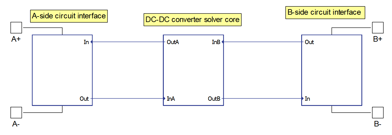
A DC-DC converter solver consists of two parts:
- the DC-DC converter solver core
- the electrical circuit interface
The signals measured in the circuit interface are used as inputs to the DC-DC converter solver core. The DC-DC converter solver core then calculates the model outputs and feeds them to the sources in the circuit interface.
DC-DC converter solver core
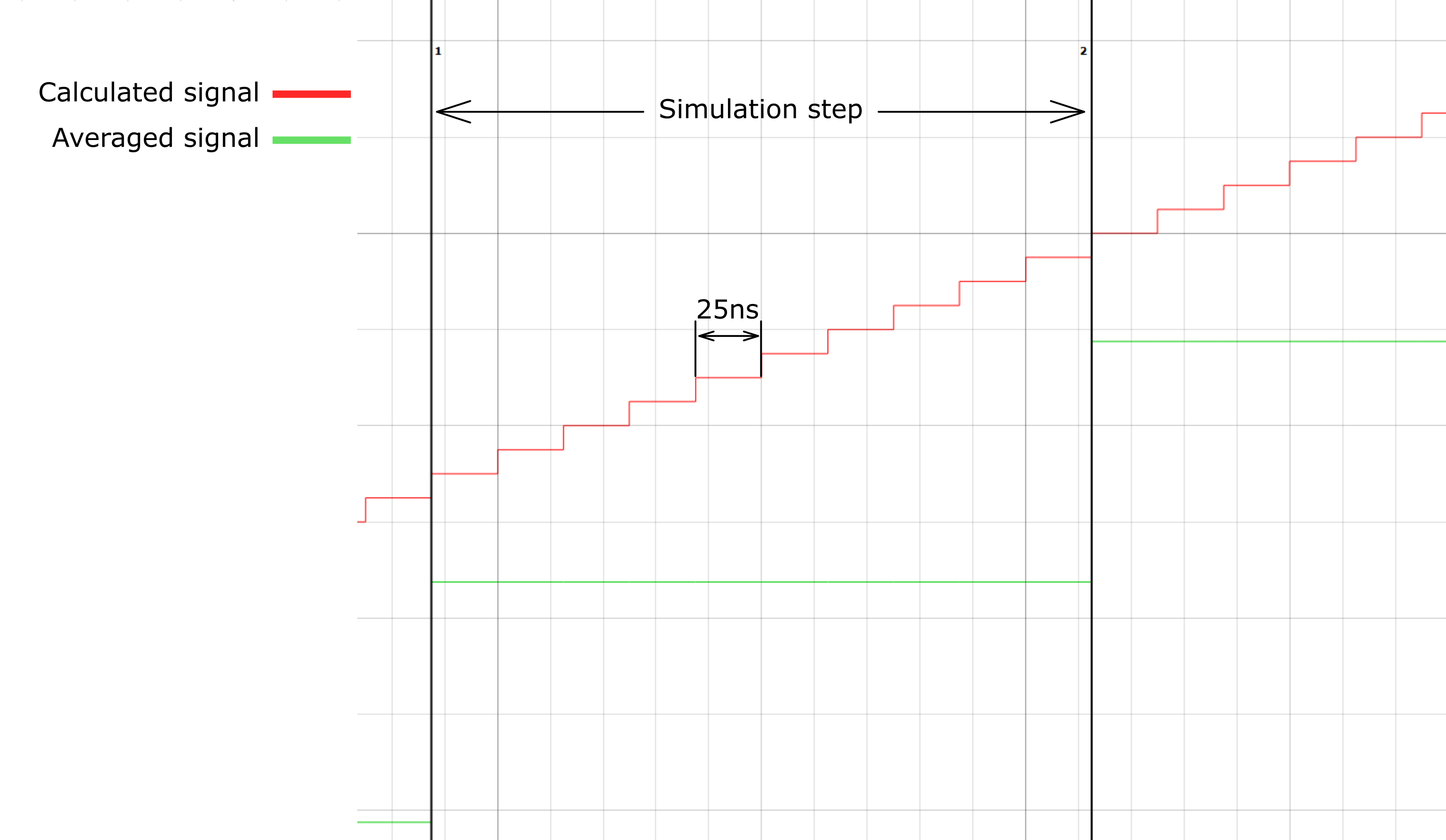
The DC-DC converter solver offers the ability to simulate the dynamics of fast-switching converter topologies with enhanced time resolution. It does so by executing part of the model with a very small time step, called the solver time step. The solver time step is fixed, in the sense that it's independent from the simulation step used for the rest of the model (configured in Table 2). At the moment, the solver simulation step is 25 ns for fourth generation devices (HIL404, HIL606), and 50 ns for third generation devices (HIL604, HIL602+). GDS oversampling is applied to all digital inputs that are used to drive the switches.
- Output sources: Signals that are injected into the circuit in order to enable the solver to interract with the rest of the model (see Electrical circuit interface).
- Measurement signals: Analog signals that are calculated by the solver (inductors' currents, capacitors' voltages, etc.). These are available in the analog signals list.
Electrical circuit interface
The DC-DC converter solver is an independent module on the FPGA. In Schematic Editor, the solver is instantiated as a converter block (see Converters). The converter component is configured like any other converter component and it invokes the solver automatically. No additional solver-specific configuration is needed.
In order to interact with the rest of the model, measurements are used as an electrical input, while controlled sources are used as solver outputs, as shown in Figure 2. The electrical circuit interface depends on the topology that is being simulated using the DC-DC converter solver. In some cases measurements are voltage measurements and sources are current sources, while in other cases it is the opposite. Interface specifics for the topology that is being simulated is described in the documentation of that converter topology. The electrical circuit interface should be taken into consideration when using converters that are based upon the DC-DC converter solver, in order to avoid potential Topological Conflicts. Additionally, electrical circuit interface subcircuits (A-side and B-side) are decoupled, meaning that they are placed into separate SPC cores, unless specified otherwise, using a Core marker component.