Flying Capacitor Boost Converter
Description of the Flying Capacitor Boost converter component in Schematic Editor.
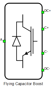
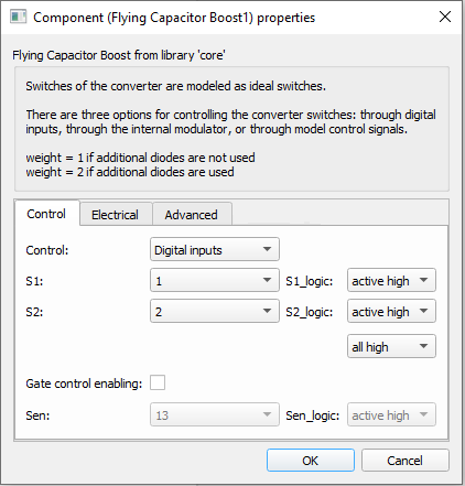
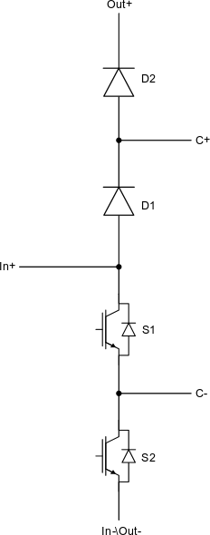
A block diagram and input parameters for the flying-capacitor boost converter block are given in Table 1.
| component | component dialog window | component parameter tabs |
|---|---|---|
|
 |
|
A schematic block diagram of the buck switching block is given in Figure 1 with corresponding switch arrangement and naming.
Digital inputs, when selected as the Control parameter, enables you to assign gate drive inputs to any of the digital input pins (from 1 to 32). For example, if S1 is assigned to 1, the digital input pin 1 will be routed to the S1 switch gate drive. In addition, the gate_logic parameter is set to either active high (i.e. high-level input voltage VIH which turns on the switch) or active low (i.e. low-level input voltage VIL which turns on the switch). The gate drive logic depends on your external controller design.
The Internal modulator, when selected as the Control parameter, enables you to use the internal PWM modulator for driving the S1 switch instead of the digital input pins. In this configuration, three additional component inputs will be present. The En input is used to enable/disable PWM modulator control, while In1 and In2 are used as the reference signal input for the internal PWM modulator. There are two PWM modulators with a 180 degree phase shift between their corresponding triangular carriers. In1 is a reference signal for the PWM modulator that controls the switch S1, while In2 is a reference signal for the PWM modulator that controls the switch S2.
Model, when selected as the Control parameter, enables you to set the IGBT gate drive signal directly from the signal processing model. The input pin gate appears on the component. It is a 2-element vectorized input, where the first value controls the S1 switch gate and the second value controls the S2 switch gate. When controlled from the model, the logic is always set to active high.
Additional diodes
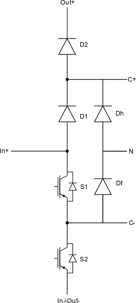
The Electrical tab allows for the use of two additional diodes in the schematic. If the checkbox is not checked, the internal schematic block diagram of the converter is shown in Figure 1. If the option is enabled, the diodes are added to the schematic, as shown in Figure 2. If the diodes are added, the converter weight is 2, otherwise it is 1.
PESB Optimization
The PESB Optimization option is available in certain converter models. When PESB Optimization is enabled, all converter's short circuit state space modes will be merged and treated as the same state space mode. For example, if one converter leg within the three phase converter is short circuited and PESB Optimization is enabled, all of the legs within the three phase converter will also be short circuited. This simplification for short circuit modeling can save a significant amount of matrix memory.
Digital Alias
If a converter is controlled by digital inputs, an alias for every digital input used by the converter will be created. Digital input aliases will be available under the Digital inputs list alongside existing Digital input signals. The alias will be shown as Converter_name.Switch_name, where Converter_name is name of the converter component and Switch_name is name of the controllable switch in the converter.