Back to back converter
Description of the Switching and Average Back to Back converter components, implemented with a current control loop.
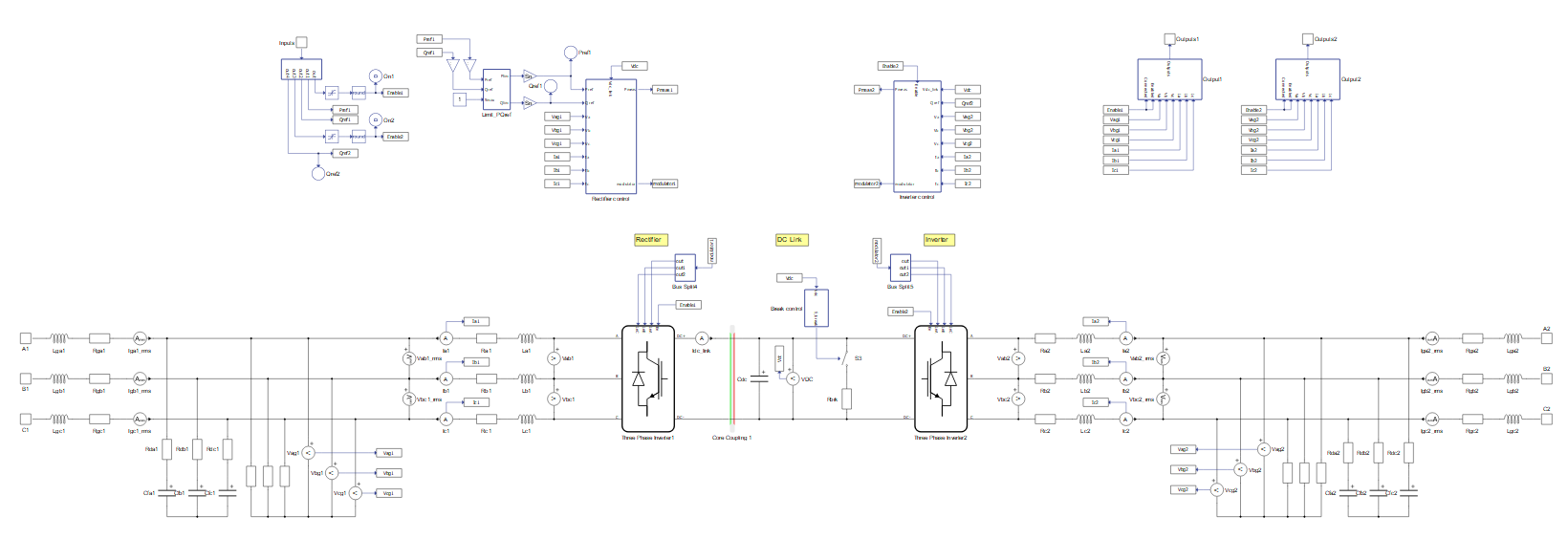
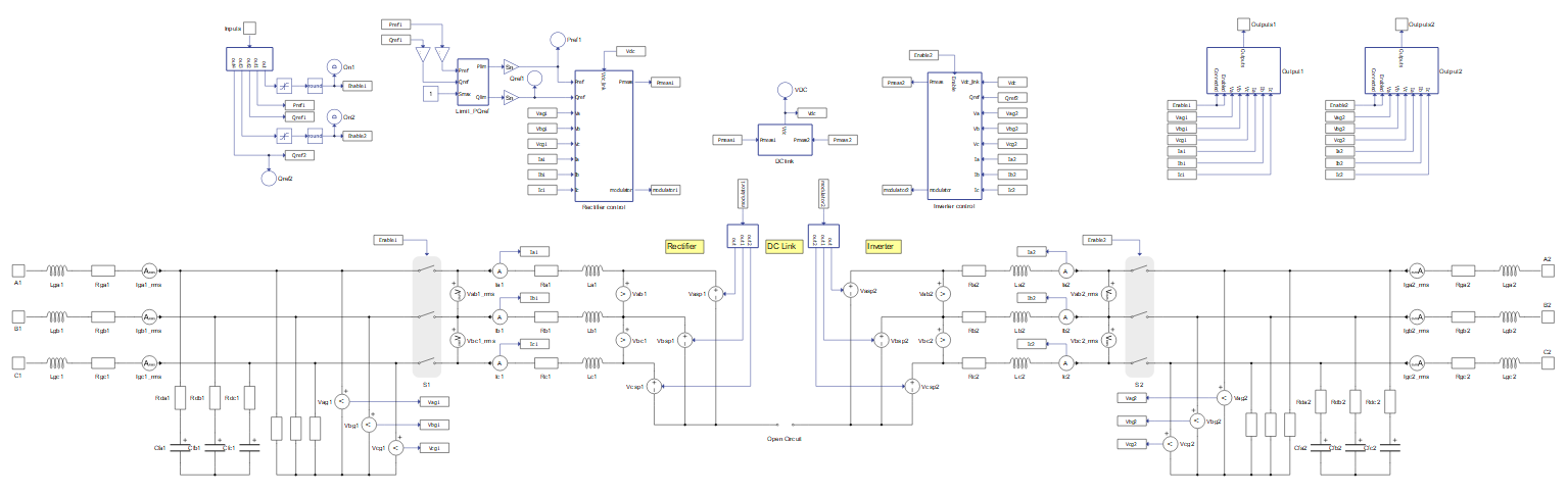
The Schematic Editor library block from the Microgrid section shown in Table 1, models a back to back converter implemented with current control loop. One of the inverters of the converter is responsible for the DC link voltage control while the other is responsible for the active power flux through the converter. This back to back converter can only operate as grid following on both sides of the converter. This converter is implemented in both switching and average models. The following sections describe in more details the component parameters, inputs and outputs.
| component | component dialog window | component parameters |
|---|---|---|
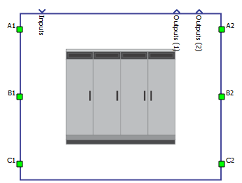 Back to Back Converter (Switching/Average) |
 |
|
Inputs and outputs
The back to back converter component needs 5 inputs to operate. These inputs must be sent as an array, with use of a Bus Join component, and in the correct order. Table 2 describes the inputs and their order.
| Number | Input | Description |
|---|---|---|
| 0 | Enable1 | A digital input that commands the On/Off state of the inverter on side 1. Inverter is on when input is high. |
| 1 | Pref1 | An analog input that sets the active power reference of the inverter on side 1. [W] |
| 2 | Qref1 | An analog input that sets the reactive power reference of the inverter on side 1. [VAr] |
| 3 | Enable2 | A digital input that commands the On/Off state of the inverter on side 2. Inverter is on when input is high. |
| 4 | Qref2 | An analog input that sets the reactive power reference of the inverter on side 2. [VAr] |
The back to back converter component has 28 outputs divided equally in two arrays. Both arrays are equal in dimension and order. The Output (1) refers to the inverter on side 1, while the Output (2) refers to the inverter on side 2. The outputs are organized as arrays and can be accessed individually through a Bus Split component, respecting the correct order. Table 3 describes the outputs and their order.
| Number | Output | Description |
|---|---|---|
| 0 | Connected | A digital output with a feedback of the battery inverter contactor's state. Contactor is closed when output is high. |
| 1 | Inv_On | A digital output with a feedback of the inverter on/off state. |
| 2 | Va | An analog output with the instantaneous measurement of the inverter's phase A terminal voltage. [V] |
| 3 | Vb | An analog output with the instantaneous measurement of the inverter's phase B terminal voltage. [V] |
| 4 | Vc | An analog output with the instantaneous measurement of the inverter's phase C terminal voltage. [V] |
| 5 | Vt | An analog output with the inverter's terminal peak voltage (phase to neutral). [V]; The RMS voltage can be calculated by dividing this output by a square root of 2. |
| 6 | Ia | An analog output with the instantaneous measurement of the inverter's phase A terminal current. [A] |
| 7 | Ib | An analog output with the instantaneous measurement of the inverter's phase B terminal current. [A] |
| 8 | Ic | An analog output with the instantaneous measurement of the inverter's phase C terminal current. [A] |
| 9 | f | An analog output with the measured electrical frequency. [Hz] |
| 10 | P | An analog output with the inverter's active power measurement. [W] |
| 11 | Q | An analog output with the inverter's reactive power measurement. [VAr] |
| 12 | S | An analog output with the inverter's apparent power measurement. [VA] |
| 13 | pf | An analog output with the inverter's power factor measurement. |
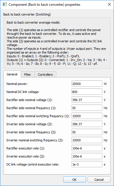
Component dialogue box and parameters
The back to back converter component dialogue box consists of 3 tabs for specifying basic and advanced parameters.
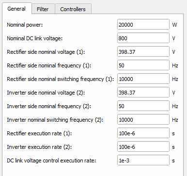
Tab: "General"
In this component tab, you can specify general parameters of the back to back converter model.
| Parameter | Code name | Description |
|---|---|---|
| Nominal power | Sn | Back to back converter nominal power. [VA] |
| Nominal DC link voltage | Vdc | Back to back converter nominal DC link voltage. [V] |
| Rectifier side nominal voltage (1) | Vn1 | Back to back converter side 1 nominal voltage. [V] |
| Rectifier side nominal frequency (1) | f1 | Back to back converter side 1 nominal electrical frequency. [Hz] |
| Rectifier side switching frequency (1) | fsw1 | Back to back converter side 1 switching frequency. [Hz] |
| Inverter side nominal voltage (2) | Vn2 | Back to back converter side 2 nominal voltage. [V] |
| Inverter side nominal frequency (2) | f2 | Back to back converter side 2 nominal electrical frequency. [Hz] |
| Inverter side switching frequency (2) | fsw2 | Back to back converter side 2 switching frequency. [Hz] |
| Rectifier execution rate (1) | Ts1 | Execution rate of all signal processing components on the side 1 of the back to back converter. [s] |
| Inverter execution rate (2) | Ts1 | Execution rate of all signal processing components on the side 2 of the back to back converter. [s] |
| DC link voltage control execution rate | Tslow | Execution rate of the DC link voltage control of the back to back converter. [s] |
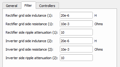
Tab: "Filter"
In this component tab, you can specify LCL filter parameters of the back to back converter model.
| Parameter | Code name | Description |
|---|---|---|
| Rectifier grid side inductance (1) | Lg1 | Inductor of the LCL filter on the grid side 1. [H] |
| Rectifier grid side resistance (1) | Rg1 | Series resistor of the inductors on the grid side 1. [Ω] |
| Rectifier ripple attenuation (1) | a1 | Attenuation constant used to calculate the filter impedances for the inverter on side 1. |
| Inverter grid side inductance (2) | Lg2 | Inductor of the LCL filter on the grid side 2. [H] |
| Inverter grid side resistance (2) | Rg2 | Series resistor of the inductors on the grid side 2. [Ω] |
| Inverter ripple attenuation (2) | a2 | Attenuation constant used to calculate the filter impedances for the inverter on side 2. |
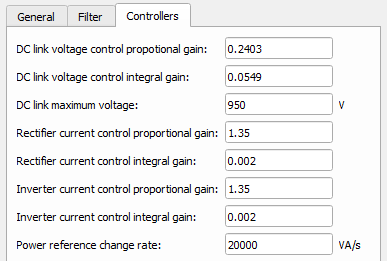
Tab: "Controllers"
In this component tab, you can specify controller parameters of the back to back converter model.
| Parameter | Code name | Description |
|---|---|---|
| DC link voltage control proportional gain | kp_v | DC link voltage PI controller proportional gain. |
| DC link voltage control integral gain | ki_v | DC link voltage PI controller integral gain. |
| DC link maximum voltage | Vdc_max | Maximum allowed voltage on the DC link. [V] |
| Rectifier current control proportional gain (1) | kp1 | Rectifier current PI controller proportional gain (1). |
| Rectifier current control integral gain (1) | ki1 | Rectifier current PI controller integral gain (1). |
| Inverter current control proportional gain (2) | kp2 | Inverter current PI controller proportional gain (2). |
| Inverter current control integral gain (2) | ki2 | Inverter current PI controller integral gain (2). |
| Power reference change rate | powerRate | Power reference rate of change [VA/s] |
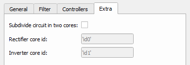
Tab: "Extra"
The Extra tab is only available in the back to back converter average model. This property is used to divide the converter across two cores.
| Parameter | Code name | Description |
|---|---|---|
| Subdivide circuit in two cores | core_div | A check box that enables core division in the DC link if checked. |
| Rectifier core id | rect_id | Identification for the core on the rectifier side (1). |
| Inverter core id | inv_id | Identification for the core on the inverter side (2). |
Example
Overall behavior and control methodologies can be better understood with the use of the given back to back converter example:
Model name: back_to_back_converter.tse and back_to_back_converter_avg.tse
SCADA interface: SCADA_Panel.cus
Path: /examples/models/microgrid/back_to_back converter/
Folder: /back_to_back (switching)/ and /back_to_back (average)/