Device couplings - Ideal Transformer
This section describes device couplings
 These components are ignored in TyphoonSim. Offline simulators,
like TyphoonSim, use variable simulation step in their simulations, so the real-time
constraints are not a concern. As a result, model partitioning is not required for offline
simulations because there is no need to split the model to improve computational performance
within a fixed time frame. The component will remain connected, but it will be bypassed.
These components are ignored in TyphoonSim. Offline simulators,
like TyphoonSim, use variable simulation step in their simulations, so the real-time
constraints are not a concern. As a result, model partitioning is not required for offline
simulations because there is no need to split the model to improve computational performance
within a fixed time frame. The component will remain connected, but it will be bypassed.
Device coupling components are ideal transformers with a transfer ratio of one. They are used to partition the complete power electronics circuit into separate circuits that are emulated on different HIL devices. These components are only used in multi-HIL configurations where HIL devices are paralleled. Device coupling components define the communication variables between HIL devices, that are exchanged through High Speed Serial Link (HSSL). This ideal transformer block introduces a variable time delay between measured variables and corresponding controlled sources, which is negligible for most practical systems. The inherent paralleling link delay between two directly connected devices is ~0.5 µs, while total delay depends on several factors, including the amount of data that has to be transmitted through HSSL, the simulation timestep, the number of devices in paralleling chain, i.e., if devices exchanging the variable values are connected directly or through other devices in the chain, etc. The total delay between two directly connected devices can be estimated as:
Where Ts is the timestep period, the value of n is 0.5 µs when Ts is ≤ 0.5 µs or 0 otherwise, and m is a value in range [2,4].
For more details about coupling placement please refer to Coupling component placement and parametrization - Ideal Transformer based couplings.
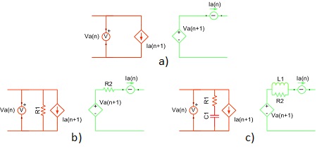
When coupling components are added to the circuit topological conflicts can occur (described in Topological Conflicts). These conflicts are solved by adding snubber circuits in parallel with the coupling's current source and/or in series with the coupling's voltage source. Snubbers are embedded in coupling components. If the Fixed snubber parameter is set to False, then snubbers are used only when there are topological issues. If the Fixed snubber parameter is set to True, the chosen snubbers will always be in the circuit.
There are three options for snubbers for both the voltage and current source sides:
- without snubber - "none"
- resistive - "R1" and "R2"
- first order filter - "R1-C1" (resistance in series with capacitor)- "R2||L1"(resistance in parallel with an inductor)
In Figure 1, a coupling building block with and without snubbers is shown.
Ports
- a_in (electrical)
- Current source side input port A for Single Phase Device Coupling.
- Current source side phase A input port for Three Phase Device Coupling and Four Phase Device Coupling.
- b_in (electrical)
- Current source side input port B for Single Phase Device Coupling.
- Current source side phase B input port for Three Phase Device Coupling and Four Phase Device Coupling.
- c_in (electrical)
- Available on Three Phase Device Coupling and Four Phase Device Coupling.
- Current source side phase C input port.
- d_in (electrical)
- Available on Four Phase Device Coupling.
- Current source side phase D input port.
- a_out (electrical)
- Current source side output port A for Single Phase Device Coupling.
- Current source side phase A output port for Three Phase Device Coupling and Four Phase Device Coupling.
- b_out (electrical)
- Current source side output port B for Single Phase Device Coupling.
- Current source side phase B output port for Three Phase Device Coupling and Four Phase Device Coupling.
- c_out (electrical)
- Available on Three Phase Device Coupling and Four Phase Device Coupling.
- Current source side phase C output port.
- d_out (electrical)
- Available on Four Phase Device Coupling.
- Current source side phase D output port.
Current source side (Tab)
- Snubber type
- Specifies type of embedded snubber - none, R1 or R1-C1.
- R1
- Available if Snubber type is set to R1 or R1-C1
- Current source side resistance [Ω].
- C1
- Available if Snubber type is set to R1-C1
- Current source side capacitance [F].
- Fixed snubber
- Available if Snubber type is set to R1 or R1-C1
- Determines whether fixed or dynamic snubber is used on current source side See fixed snubber description.
Voltage source side (Tab)
- Snubber type
- Specifies type of embedded snubber - none, R2 or R2||L1.
- R2
- Available if Snubber type is set to R2.
- Voltage source side resistance [Ω].
- L1
- Available if Snubber type is set to R2||L1
- Voltage source side inductance [H].
- Fixed snubber
- Available if Snubber type is set to R2 or R2||L1
- Specifies whether fixed or dynamic snubber is used on current source side See fixed snubber description.
Single Phase Device Coupling

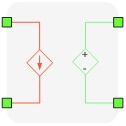
A single phase device coupling component is an ideal transformer with a transfer ratio of one, used to divide the simulated circuit into two sub-circuits. Consequently, the two sub-circuits are distributed and executed in two separate HIL devices. In addition, this ideal transformer introduces a time delay between measured variables and corresponding controlled sources, which is negligible for most practical systems.
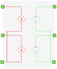
Three Phase Device Coupling

A three phase device coupling component is of two ideal transformers as shown in Figure 5 with a transfer ratio of one, used to divide the simulated circuit into two sub-circuits. Consequently, the two sub-circuits are distributed and executed in two separate HIL devices. In addition, these ideal transformers introduce a time delay between measured variables and corresponding controlled sources, which is negligible for most practical systems.
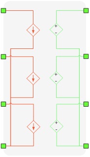
Four Phase Device Coupling

The four phase device coupling component is made of three ideal transformers as shown in Figure 7 with a transfer ratio of one, used to divide the simulated circuit into two sub-circuits. Consequently, the two sub-circuits are distributed and executed in two separate HIL devices. In addition, these ideal transformers introduce a time delay between measured variables and corresponding controlled sources, which is negligible for most practical systems.