Loop-back Latency
Description of the overall loop-back latency with a focus on digital input to analog output latency.
Loop-back Latency Overview
The overall loop-back latency is a function of the selected simulation step, model settings and component parameters, and the used device. In this section, the minimum and maximum loop-back latency cases are presented, delays within the system are explained, and hints on how to reduce latency are given.
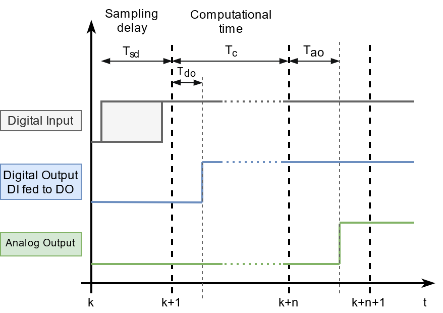
In Figure 1 a general case for loop-back latency is presented. In practical power electronics applications, the most significant parameter is the loop-back latency from the digital inputs to the analog outputs. It consists of three parts:
- Sampling delay (Tsd) - Digital inputs are continuously sampled throughout the simulation cycle. A change in the digital input signal can occur anywhere during that time and it will be applied in the next simulation cycle. The worst case scenario is when a change on the digital inputs occurs at the beginning of the simulation cycle resulting in larger sampling latency, whereas digital input changes closer to the end of the simulation cycle result in lower latency. So, the sampling delay can be anywhere between 0 and the simulation time step, depending on when the digital input event occurs relative to the simulation cycle boundaries.
- Computational time (Tc) - Time needed to calculate the model response. This time is always an integer multiple of the simulation step, ranging from 1 simulation step to several depending on the specific use case.
- Hardware output stage latency - This latency represents the time needed to propagate sampled and/or calculated values to the digital and analog outputs. It is device specific and independent of the selected simulation step. Most significant delays are the digital output delay Tdo and the analog output delay Tao. More information is available in the IO Timing section of each HIL Simulator device's documentation.
The digital output signal presented in Figure 1 is a direct feedthrough of a digital input, therefore its latency is only due to sampling uncertainty and the delay of digital output stage. For this reason, this case will not be described further.
Both maximum sampling delay and calculation time are a function of the selected simulation step value. So in general, smaller simulation steps result in lower latency and vice versa.
Minimum Loop Back Latency
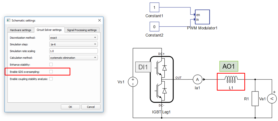
Computational time is influenced by certain model settings and component properties and can be as low as a single simulation step. The list below describes the model configuration that results in minimum digital input to analog output latency. The model used during the measurements and its relevant settings are shown in Figure 2.
System setup:
- Gate drive signals are connected to digital inputs 1 and 2 for the top and bottom switches respectively.
- Inductor current L1 is set at analog output 1 - It is important to note that L1 was used directly, and not Ia1, in order to get the minimum latency. It is possible to use Ia1 as well by setting the Exact measurement option to True.
- GDS oversampling disabled - This adds an additional simulation cycle of latency when enabled, so it is disabled here.
- Loop-back latency is measured from the event on digital input 1 to the response on analog output 1.
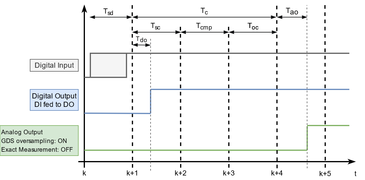
Results obtained during the test are shown in Figure 3. The figure shows the three major components of the total loop-back latency:
- Tsd - sampling delay as described above.
- Tc - calculation time. In this case it includes only the state calculation step (Tsc) and is equal to a single simulation step Ts.
- Tao - analog output latency as described above.
Overall latency is the sum of these three. Due to the sampling uncertainty, it is within the following range:
Maximum loop-back latency case
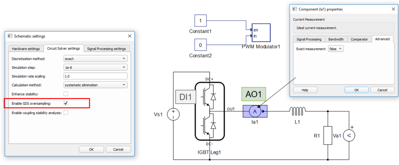
In this section, the maximum loop-back latency case is presented. The model used during the test is the same as for the minimal loop-back latency test case, while the model settings and certain component properties are modified. Relevant changes in the settings are highlighted in Figure 4.
System setup:
- Gate drive signals are connected to digital inputs 1 and 2 for the top and bottom switches respectively.
- Current measurement Ia1 is set at analog output 1
- Current measurement parameter Exact measurement is set to False.
- GDS oversampling enabled - This adds an additional simulation cycle of latency.
- Loop-back latency measured from the event on digital input 1 to the response on analog output 1.
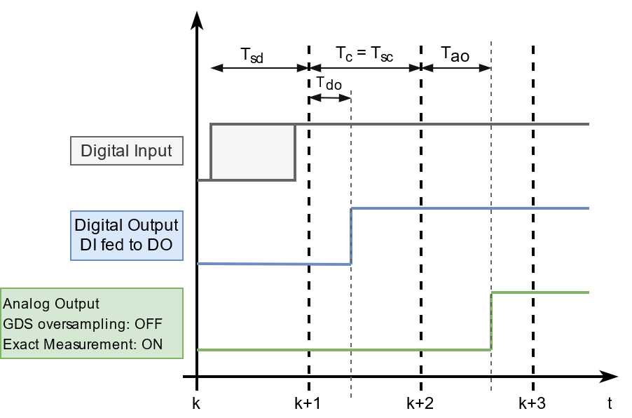
Results obtained during the test are shown in Figure 5. The figure shows all the contributing factors to the overall latency:
- Tsd - sampling delay.
- Tc - calculation time. In this case it consists of three steps:
- Tsc - state calculation time, equal to the simulation time step.
- Tcmp - state compensation time, equal to the simulation time step. Applies only when GDS oversampling is enabled.
- Toc - output calculation time, equal to the simulation time step. Applies only if the Exact measurement option in the measurement properties is disabled.
- Tao - latency of the analog output.
Overall latency is the sum of these five. Due to sampling uncertainty, it is within the following range: