Max output resistance load at max voltage output before distortion
600 Ω @ 14.142 VRMS
N/A
Input to output propagation delay
5 µs @ ±20 V; 10 kHz
Bandwidth (-3dB)
100 kHz
Max capacitive load
33 nF @ 100 kHz
Isolation
Yes
No
Table 3. Hardware Specification - Analog Input Channels
Parameter
Value
Type
Single-ended
Gain
0.4166
Number of channels
16 (see note)
Input signal range
±24 V or ±20 mA (selected with a switch)
Output signal range
±10 V
Bandwidth (-3dB)
DC to 100 kHz
Max capacitive load
33 nF @ 100 kHz
Isolation
No
Note: In the standard configuration, 2 of the channels cannot be used since they are occupied by the excitation channels.
Configurability
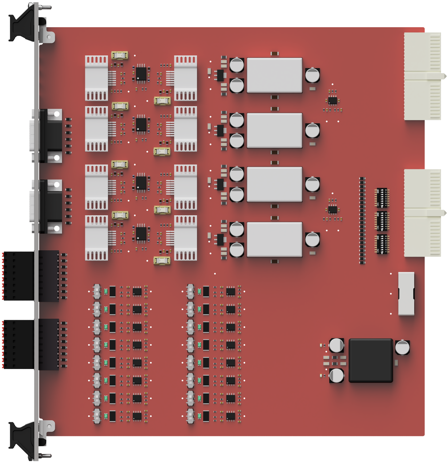
In the standard configuration, the Dual Resolver Card is configured to operate in a mode
where four analog outputs (AO1, AO2, AO3 and AO4) and two analog inputs (AI1 and AI2)
are reserved for use with two resolver channels. Thus, limiting the use of these analog I/O
channels for different purposes.
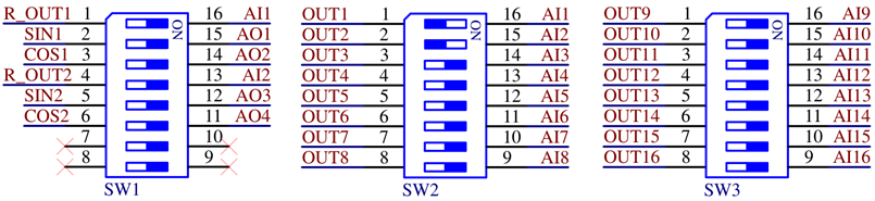
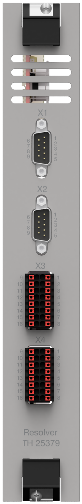
Configuration switches are available on the board and can be reconfigured if different needs
arise, as shown in Figure 2. On switches SW1 and SW3, all positions are in the ON position, as well as on switch
SW2 except positions 1 and 2 which are in the OFF position (AI1 and AI2), which allows them
to be used for resolver channels.
Figure 2. Default switch configurations (SW1, SW2, and SW3)
Analog input channels provide additional configuration options, namely the selection of the
input type between the ±24 V and ±20 mA ranges. This option is provided for each channel
separately via dedicated switches (S1 in schematic) on the board.
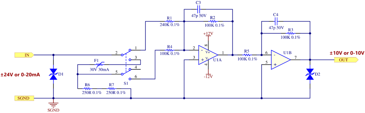
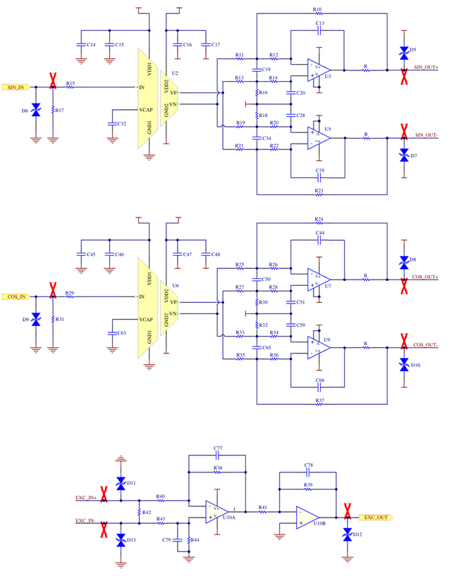
Simplified Schematics
Figure 3 and Figure 4 show simplified schematics of the Resolver Stage channel and the Analog Input channel, respectively.