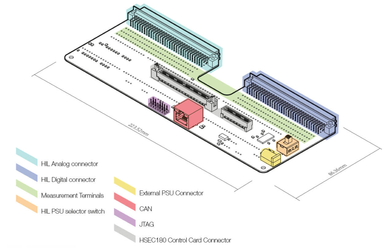
Detailed description
Detailed description of the HIL DSP 180 Interface
The board features the following key sections, as shown in Figure 1.
- HIL Analog connector
- HIL Digital connector
- HSEC 180 card connector
- Power supply
- CAN bus connector
- JTAG connector
HIL Analog I/O
Up to 24 analog outputs (AOs), and up to 3 analog inputs (AIs), are routed from the DIN41612 socket (HIL side) to the HSEC 180 connector (DSP side).
To protect against overvoltage conditions, HIL analog outputs feature series 120 Ω RZ1-RZ24 resistors that, together with TI controlCARD ADC protection diodes (U6-U11), act as a 0-3.3 V clamping circuit.
| HIL Analog Output | DSP signal |
|---|---|
| AO1/AI1* | ADC–A0/DAC-A |
|
AO2/AI2* |
ADC–A1/DAC-B |
| AO3 | ADC–A2 |
| AO4 | ADC–A3 |
| AO5 | ADC–A4 |
| AO6 | ADC–A5 |
| AO7 | ADC–14 |
| AO8 | ADC–15 |
| AO9 | ADC–B0 |
| AO10/AI3* | ADC-B1/DAC-C |
| AO11 | ADC–B2 |
| AO12 | ADC–B3 |
| AO13 | ADC–B4 |
| AO14 | ADC–B5 |
| AO15 | ADC–D0 |
| AO16 | ADC–D1 |
| AO17 | ADC-C2 |
| AO18 | ADC-C3 |
| AO19 | ADC-C4 |
| AO20 | ADC-C5 |
| AO21 | ADC-D2 |
| AO22 | ADC-D3 |
| AO23 | ADC-D4 |
| AO24 | ADC-D5 |
* Depending on the position of the R25, R26, or R27 jumpers, this HIL AO or HIL AI may be routed to the DSP analog pin. By default, HIL AOs are routed to the DSP ADC.
HIL Digital I/O
Up to 16 digital outputs, and 24 digital inputs, are routed to the GPIO ports of the corresponding controlCARD.
| HIL Digital Output signal | DSP Digital Input signal |
|---|---|
| DO1 | GPIO-54/QEP-2A |
| DO2 |
GPIO-55/QEP-2B |
| DO3 | GPIO-56/QEP-2S |
| DO4 | GPIO-57/QEP-2I |
| DO5 | GPIO-50 |
| DO6 | GPIO-51 |
| DO7 | GPIO-52 |
| DO8 | GPIO-53 |
| DO9 | GPIO-35 |
| DO10 | GPIO-36 |
| DO11 | GPIO-37 |
| DO12 | GPIO-38 |
| DO13 | GPIO-60 |
| DO14 | GPIO-61 |
| DO15 | GPIO-62 |
| DO16 | GPIO-63 |
| HIL Digital Input signal | DSP Digital Output signal |
|---|---|
| DI1 | GPIO-00/PWM-1A |
| DI2 | GPIO-02/PWM-2A |
| DI3 | GPIO-04/PWM-3A |
| DI4 | GPIO-06/PWM-4A |
| DI5 | GPIO-08/PWM-5A |
| DI6 | GPIO-10/PWM-6A |
| DI7 | GPIO-01/PWM-1B |
| DI8 | GPIO-03/PWM-2B |
| DI9 | GPIO-05/PWM-3B |
| DI10 | GPIO-07/PWM-4B |
| DI11 | GPIO-09/PWM-5B |
| DI12 | GPIO-11/PWM-6B |
| DI13 | GPIO-14/PWM-8A |
| DI14 | GPIO-12/PWM-7A |
| DI15 | GPIO-15/PWM-8B |
| DI16 | GPIO-13/PWM-7B |
| DI17 | GPIO-34 |
| DI18 | GPIO-39 |
| DI19 | GPIO-40 |
| DI20 | GPIO-41 |
| DI21 | GPIO-44 |
| DI22 | GPIO-45 |
| DI23 | GPIO-48 |
| DI24 | GPIO-49 |
HSEC 180 Connector
The HSEC 180 connector is a standardized connector for Texas Instruments 180 pin controlCARD modules. The following controlCARD modules are supported without any modifications:
Power Supply
The DSP 180 Interface is powered by a 5 V rail, supplied directly from HIL User PSU section, or from the onboard 5 V buck regulator (powered externally from a 12 V DC power supply).
For use cases when the controlCARD is used separately from the HIL, in a standalone configuration, it is possible to configure the HIL DSP 180 Interface Board to be powered from an external power source, via an onboard selector switch. This turns the HIL DSP180 Interface Board into a generic controlCARD development board.
When this selector switch, labeled DSP PWR, is in the "HIL" position, the 5 V rail of TI controlCARD is supplied directly from the HIL 5 V rail. In this mode, no external adapter is required.
- PGOOD (ON when rail is lower than 5 V or output current higher than 1 A)
- PWR (ON when 5 V rail is present)
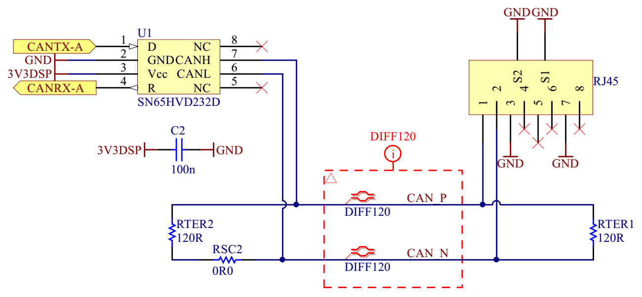
CAN bus
The controlCARD DSP’s CAN-A module (GPIO-30/CANRX-A and GPIO-31/CANTX-A) is connected to the onboard CAN transceiver, SN65HVD232D from Texas Instruments, which forms the 3.3 V CAN bus as shown on the Figure 2.
The CAN bus is accessible over the RJ45 connector and it is terminated with two 120 Ω resistors. If the external 3.3 V CAN bus is connected to the HIL DSP 180 Interface CAN bus, care must be taken to remove the redundant terminating resistors on both buses. On the DSP 180 Interface, this is done by removing the RSC2 (0 Ω) resistor.
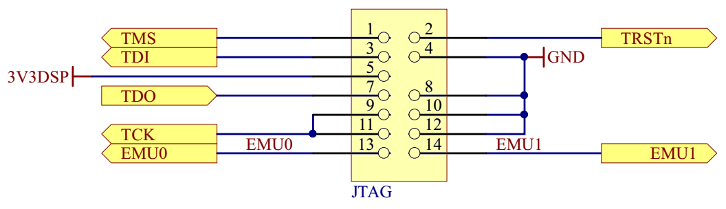
JTAG
The JTAG section consists of the JTAG header, with a pinout shown on the Figure 3.
“Texas Instruments“ and “TI“ are registered trademarks of Texas Instruments Incorporated in the United States of America, or other countries, or both.