Detailed description
Detailed description of the HIL Power Link Interface
Layout
The interface includes the following segments, as shown in Figure 1.
- 5-24 V DC Power supply Input
- GPIO connectors, 5 V rating
- 4 Optical Channels (4x TX, 4x RX), DC to 50 MBd rating, Isolated
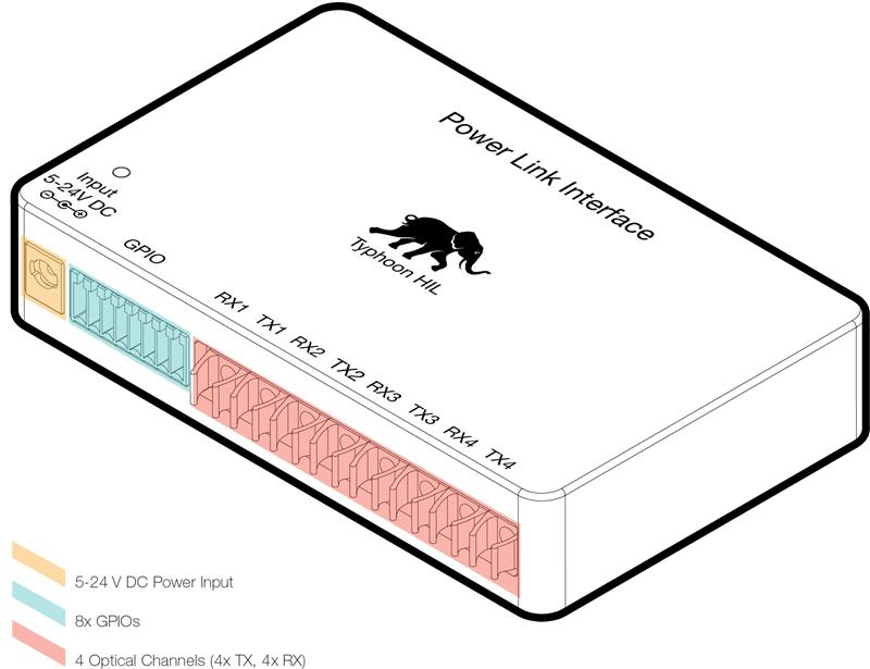
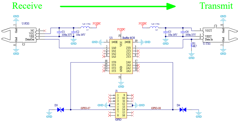
Figure 2 shows an example of communication on one channel, representing 1 receive and 1 transmit module, connected through the buffer on the GPIO connector.
Connector Pinout
Table 1 shows the pinout between the HIL GPIO and the HIL Power Link interface when using the provided HIL Power Link custom cable.
Note: The GPIO pinout on the HIL device is inverted relative to the HIL Power Link
Interface connector, so it is recommended to use the provided cable.
| GPIO Pin | Optical Channel | Interface diagram |
|---|---|---|
| GPIO 1 | RX1 | 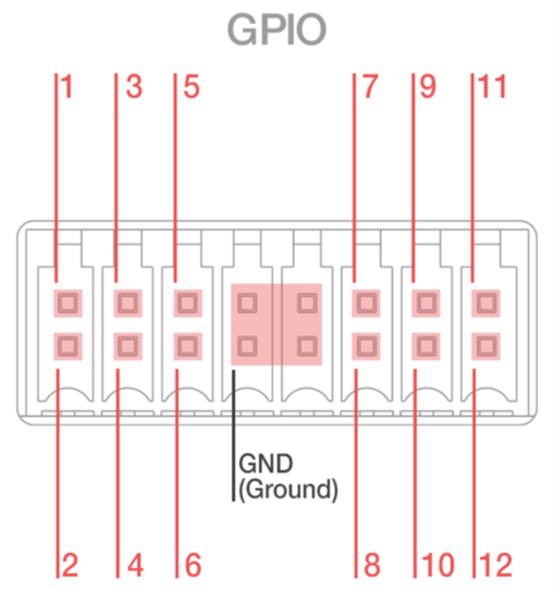 |
| GPIO 2 | TX1 | |
| GPIO 3 | RX2 | |
| GPIO 4 | TX2 | |
| GPIO 5 | RX3 | |
| GPIO 6 | TX3 | |
| GPIO 7 | RX4 | |
| GPIO 8 | TX4 |