IO Timing
Sample rates and timing details for HIL404 devices
IO Timing Details
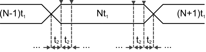
All analog IOs are updated/sampled at the beginning of each simulation time step (t1), which is software defined. To improve the PWM sampling resolution, digital inputs actually are sampled at a higher rate (t2), independent of the simulation time step value. Similarly, digital outputs are updated at a higher t2 rate. For overall expected loop-back latency, please consult Loopback Latency.
| Symbol | Parameter | Value |
|---|---|---|
| t1 | Simulation step | Software defined |
| t2 | Digital input sampling time | 280 MSPS |
| IO class | Sample/Update rate | Comment |
|---|---|---|
| Digital input | 280 MSPS | All digital inputs are sampled simultaneously. |
| Digital output | Up to 280 MSPS | All digital outputs are updated simultaneously. |
| Analog input | 1/t1 | All analog inputs are sampled simultaneously. Minimum sample time is 1μs |
| Analog output | 1/t1* | All analog outputs are updated simultaneously. |
*Valid for all simulation timesteps except 200 ns; in this case, all analog outputs are updated on every other time step (400 ns).
| IO class | HIL404 |
|---|---|
| Digital output (Tdo) | 150 ns |
| Analog output (Tao) | 340 ns |